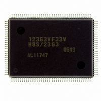
D12363VF33V Renesas Electronics America, D12363VF33V Datasheet - Page 729

D12363VF33V
Manufacturer Part Number
D12363VF33V
Description
IC H8S/2363 MCU ROMLESS 128QFP
Manufacturer
Renesas Electronics America
Series
H8® H8S/2300r
Specifications of D12363VF33V
Core Processor
H8S/2000
Core Size
16-Bit
Speed
33MHz
Connectivity
I²C, IrDA, SCI, SmartCard
Peripherals
DMA, POR, PWM, WDT
Number Of I /o
84
Program Memory Type
ROMless
Ram Size
16K x 8
Voltage - Supply (vcc/vdd)
3 V ~ 3.6 V
Data Converters
A/D 10x10b, D/A 2x8b
Oscillator Type
Internal
Operating Temperature
-20°C ~ 75°C
Package / Case
128-QFP
For Use With
YR0K42378FC000BA - KIT EVAL FOR H8S/2378
Lead Free Status / RoHS Status
Lead free / RoHS Compliant
Eeprom Size
-
Program Memory Size
-
Available stocks
Company
Part Number
Manufacturer
Quantity
Price
Company:
Part Number:
D12363VF33V
Manufacturer:
ST
Quantity:
67 000
Company:
Part Number:
D12363VF33V
Manufacturer:
Renesas Electronics America
Quantity:
10 000
Part Number:
D12363VF33V
Manufacturer:
RENSAS
Quantity:
20 000
- Current page: 729 of 1044
- Download datasheet (6Mb)
16.4
The A/D converter operates by successive approximation with 10-bit resolution. It has two
operating modes: single mode and scan mode. When changing the operating mode or analog input
channel, to prevent incorrect operation, first clear the bit ADST to 0 in ADCSR to halt A/D
conversion. The ADST bit can be set at the same time as the operating mode or analog input
channel is changed.
16.4.1
In single mode, A/D conversion is to be performed only once on the specified single channel.
Operations are as follows.
1. A/D conversion is started when the ADST bit in ADCSR is set to 1, according to the software
2. When A/D conversion is completed, the result is transferred to the corresponding A/D data
3. On completion of conversion, the ADF bit in ADCSR is set to 1. If the ADIE bit is set to 1 at
4. The ADST bit remains set to 1 during A/D conversion, and is automatically cleared to 0 when
16.4.2
In scan mode, A/D conversion is to be performed sequentially on the specified channels:
maximum four channels or maximum eight channels. Operations are as follows.
1. When the ADST bit in ADCSR is set to 1 by software, TPU or external trigger input, A/D
2. When A/D conversion for each channel is completed, the result is sequentially transferred to
or external trigger input.
register to the channel.
this time, an ADI interrupt request is generated.
conversion ends. When the ADST bit is cleared to 0 during A/D conversion, A/D conversion
stops and the A/D converter enters wait state.
conversion starts on the first channel in the group.
The consecutive A/D conversion on maximum four channels (SCANE and SCANS = 10) or on
maximum eight channels (SCANE and SCANS = 11) can be selected. When the consecutive
A/D conversion is performed on the four channels, the A/D conversion starts on AN0 when
CH3 = 1 and CH2 = 1, AN4 when CH3 and CH2 = 01, or AN12 when CH3 and CH2 = 11.
When the consecutive A/D conversion is performed on the eight channels, the A/D conversion
starts on AN0 when CH3 = 0.
the corresponding A/D data register to each channel.
Operation
Single Mode
Scan Mode
Rev.6.00 Mar. 18, 2009 Page 669 of 980
Section 16 A/D Converter
REJ09B0050-0600
Related parts for D12363VF33V
Image
Part Number
Description
Manufacturer
Datasheet
Request
R

Part Number:
Description:
KIT STARTER FOR M16C/29
Manufacturer:
Renesas Electronics America
Datasheet:

Part Number:
Description:
KIT STARTER FOR R8C/2D
Manufacturer:
Renesas Electronics America
Datasheet:

Part Number:
Description:
R0K33062P STARTER KIT
Manufacturer:
Renesas Electronics America
Datasheet:

Part Number:
Description:
KIT STARTER FOR R8C/23 E8A
Manufacturer:
Renesas Electronics America
Datasheet:

Part Number:
Description:
KIT STARTER FOR R8C/25
Manufacturer:
Renesas Electronics America
Datasheet:

Part Number:
Description:
KIT STARTER H8S2456 SHARPE DSPLY
Manufacturer:
Renesas Electronics America
Datasheet:

Part Number:
Description:
KIT STARTER FOR R8C38C
Manufacturer:
Renesas Electronics America
Datasheet:

Part Number:
Description:
KIT STARTER FOR R8C35C
Manufacturer:
Renesas Electronics America
Datasheet:

Part Number:
Description:
KIT STARTER FOR R8CL3AC+LCD APPS
Manufacturer:
Renesas Electronics America
Datasheet:

Part Number:
Description:
KIT STARTER FOR RX610
Manufacturer:
Renesas Electronics America
Datasheet:

Part Number:
Description:
KIT STARTER FOR R32C/118
Manufacturer:
Renesas Electronics America
Datasheet:

Part Number:
Description:
KIT DEV RSK-R8C/26-29
Manufacturer:
Renesas Electronics America
Datasheet:

Part Number:
Description:
KIT STARTER FOR SH7124
Manufacturer:
Renesas Electronics America
Datasheet:

Part Number:
Description:
KIT STARTER FOR H8SX/1622
Manufacturer:
Renesas Electronics America
Datasheet:

Part Number:
Description:
KIT DEV FOR SH7203
Manufacturer:
Renesas Electronics America
Datasheet:


