D12363VF33V Renesas Electronics America, D12363VF33V Datasheet - Page 683
D12363VF33V
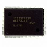
Manufacturer Part Number
D12363VF33V
Description
IC H8S/2363 MCU ROMLESS 128QFP
Manufacturer
Renesas Electronics America
Series
H8® H8S/2300r
Specifications of D12363VF33V
Core Processor
H8S/2000
Core Size
16-Bit
Speed
33MHz
Connectivity
I²C, IrDA, SCI, SmartCard
Peripherals
DMA, POR, PWM, WDT
Number Of I /o
84
Program Memory Type
ROMless
Ram Size
16K x 8
Voltage - Supply (vcc/vdd)
3 V ~ 3.6 V
Data Converters
A/D 10x10b, D/A 2x8b
Oscillator Type
Internal
Operating Temperature
-20°C ~ 75°C
Package / Case
128-QFP
For Use With
YR0K42378FC000BA - KIT EVAL FOR H8S/2378
Lead Free Status / RoHS Status
Lead free / RoHS Compliant
Eeprom Size
-
Program Memory Size
-
Available stocks
Company
Part Number
Manufacturer
Quantity
Price
Company:

Part Number:
D12363VF33V
Manufacturer:
ST
Quantity:
67 000
Company:
Part Number:
D12363VF33V
Manufacturer:
Renesas Electronics America
Quantity:
10 000
Part Number:
D12363VF33V
Manufacturer:
RENSAS
Quantity:
20 000


14.10.4 Receive Error Flags and Transmit Operations (Clocked Synchronous Mode Only)
Transmission cannot be started when a receive error flag (ORER, PER, or FER) is set to 1, even if
the TDRE flag is cleared to 0. Be sure to clear the receive error flags to 0 before starting
transmission. Note also that receive error flags cannot be cleared to 0 even if the RE bit is cleared
to 0.
14.10.5 Relation between Writes to TDR and the TDRE Flag
The TDRE flag in SSR is a status flag that indicates that transmit data has been transferred from
TDR to TSR. When the SCI transfers data from TDR to TSR, the TDRE flag is set to 1.
Data can be written to TDR regardless of the state of the TDRE flag. However, if new data is
written to TDR when the TDRE flag is cleared to 0, the data stored in TDR will be lost since it has
not yet been transferred to TSR. It is therefore essential to check that the TDRE flag is set to 1
before writing transmit data to TDR.
14.10.6 Restrictions on Use of DMAC or DTC
• When an external clock source is used as the serial clock, the transmit clock should not be
• When RDR is read by the DMAC or DTC, be sure to set the activation source to the relevant
input until at least five φ clock cycles after TDR is updated by the DMAC or DTC. Abnormal
operation may occur if the transmit clock is input within 4 φ clocks after TDR is updated.
(figure 14.35)
SCI receive-data-full interrupt (RXI).
SCK
TDRE
Serial data
Note: When operating on an external clock, set t > 4 clocks.
Figure 14.35 Example of Synchronous Transmission Using DTC
t
LSB
D0
D1
Section 14 Serial Communication Interface (SCI, IrDA)
D2
D3
Rev.6.00 Mar. 18, 2009 Page 623 of 980
D4
D5
D6
REJ09B0050-0600
D7
Related parts for D12363VF33V
Image
Part Number
Description
Manufacturer
Datasheet
Request
R

Part Number:
Description:
KIT STARTER FOR M16C/29
Manufacturer:
Renesas Electronics America
Datasheet:

Part Number:
Description:
KIT STARTER FOR R8C/2D
Manufacturer:
Renesas Electronics America
Datasheet:

Part Number:
Description:
R0K33062P STARTER KIT
Manufacturer:
Renesas Electronics America
Datasheet:

Part Number:
Description:
KIT STARTER FOR R8C/23 E8A
Manufacturer:
Renesas Electronics America
Datasheet:

Part Number:
Description:
KIT STARTER FOR R8C/25
Manufacturer:
Renesas Electronics America
Datasheet:

Part Number:
Description:
KIT STARTER H8S2456 SHARPE DSPLY
Manufacturer:
Renesas Electronics America
Datasheet:

Part Number:
Description:
KIT STARTER FOR R8C38C
Manufacturer:
Renesas Electronics America
Datasheet:

Part Number:
Description:
KIT STARTER FOR R8C35C
Manufacturer:
Renesas Electronics America
Datasheet:

Part Number:
Description:
KIT STARTER FOR R8CL3AC+LCD APPS
Manufacturer:
Renesas Electronics America
Datasheet:
Part Number:
Description:
KIT STARTER FOR RX610
Manufacturer:
Renesas Electronics America
Datasheet:

Part Number:
Description:
KIT STARTER FOR R32C/118
Manufacturer:
Renesas Electronics America
Datasheet:

Part Number:
Description:
KIT DEV RSK-R8C/26-29
Manufacturer:
Renesas Electronics America
Datasheet:

Part Number:
Description:
KIT STARTER FOR SH7124
Manufacturer:
Renesas Electronics America
Datasheet:

Part Number:
Description:
KIT STARTER FOR H8SX/1622
Manufacturer:
Renesas Electronics America
Datasheet:

Part Number:
Description:
KIT DEV FOR SH7203
Manufacturer:
Renesas Electronics America
Datasheet: