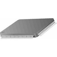
MC68HC11K0CFUE4 Freescale Semiconductor, MC68HC11K0CFUE4 Datasheet - Page 251

MC68HC11K0CFUE4
Manufacturer Part Number
MC68HC11K0CFUE4
Description
MCU 8-BIT 768 RAM 4MHZ 80-QFP
Manufacturer
Freescale Semiconductor
Series
HC11r
Specifications of MC68HC11K0CFUE4
Core Processor
HC11
Core Size
8-Bit
Speed
4MHz
Connectivity
SCI, SPI
Peripherals
POR, PWM, WDT
Number Of I /o
37
Program Memory Type
ROMless
Ram Size
768 x 8
Voltage - Supply (vcc/vdd)
4.5 V ~ 5.5 V
Data Converters
A/D 8x8b
Oscillator Type
Internal
Operating Temperature
-40°C ~ 85°C
Package / Case
80-QFP
Data Bus Width
8 bit
Data Ram Size
768 B
Interface Type
SCI, SPI
Maximum Clock Frequency
4 MHz
Number Of Programmable I/os
37
Number Of Timers
8
Maximum Operating Temperature
+ 85 C
Mounting Style
SMD/SMT
Minimum Operating Temperature
- 40 C
On-chip Adc
8 bit, 8 Channel
Lead Free Status / RoHS Status
Lead free / RoHS Compliant
Eeprom Size
-
Program Memory Size
-
Lead Free Status / Rohs Status
Details
Available stocks
Company
Part Number
Manufacturer
Quantity
Price
Company:
Part Number:
MC68HC11K0CFUE4
Manufacturer:
Freescale Semiconductor
Quantity:
10 000
- Current page: 251 of 290
- Download datasheet (4Mb)
M68HC11K Family
MOTOROLA
MMWBR = $84
$FFFF
$8000
$C000
$A000
MMSIZ = $E1
$0000
$1000
$4000
$6000
PGAR = $1F
EE/REG/RAM
INTERNAL
(EP)ROM
Memory Map for One 8-Kbyte Window with Eight Banks and
Figure 11-16. Memory Expansion Example 2 (Sheet 1 of 2)
One 16-Kbyte Window with 16 Banks of External Memory
SELECT
SELECT
XA[17:13]
Window 1 @ $4000
Window 2 @ $8000
Window 1 = 8 Kbytes
Window 2 = 16 Kbytes
GPCS1, GPCS2 based
on expansion address
CHIP
CHIP
The second example system shown in
memory windows. The first window is organized as in the previous
example, 8 banks of 8 Kbytes each. The second window accesses
256 Kbytes of memory in 16 banks of 16 Kbyte each. To access
16 Kbytes, or 2
ADDR[13:0]. Since ADDR13 is driven on XA13 in this example, XA13
replaces ADDR13 to drive the A13 line in the 6226 devices, but ADDR13
could be used as well. 16 (2
address lines, A[17:14]. Refer to
schematic drawing of this system.
1
2
Freescale Semiconductor, Inc.
XA[15:13] =
For More Information On This Product,
XA[17:14] =
$05FFF
BANK 0
$04000
$0BFFF
BANK 0
$08000
0:0:0
0:0:0:0
Memory Expansion and Chip Selects
XA[15:13] =
Go to: www.freescale.com
XA[17:14] =
$15FFF
BANK 1
$14000
BANK 1
$1BFFF
$18000
0:0:1
14
0:0:0:1
address locations, the CPU will need 14 address lines,
GPCS1C = $06
GPCS1A = $00
GPCS2A = $00
GPCS2C = $08
CSCTL = $00
XA[15:13] =
$25FFF
$24000
BANK2
XA[17:14] =
$2BFFF
0:1:0
$28000
BANK 2
0:0:1:0
XA[15:13] =
4
BANK 3
$35FFF
$34000
) memory banks require four expansion
0:1:1
XA[17:14] =
WINDOW 1
$3BFFF
WINDOW 2
BANK 3
$38000
0:0:1:1
Figure 11-16
No I/O or program chip selects
General-purpose chip select 1 from $00000
64 KByte range (8 x 8 K)
General-purpose chip select 2 from $00000
256 KByte range (16 x 16 K)
XA[15:13] =
BANK 4
$45FFF
$44000
1:0:0
XA[17:14] =
Figure 11-16
BANK 4
0:1:0:0
Memory Expansion and Chip Selects
$4BFFF
$48000
XA[15:13] =
BANK 5
$55FFF
$54000
1:0:1
Memory Expansion Examples
for a memory map and
XA[15:13] =
$65FFF
$64000
BANK6
1:1:0
contains two
XA[15:13] =
XA[17:14] =
BANK 7
$75FFF
$74000
Technical Data
BANK 15
$FBFFF
$F8000
1:1:1
1:1:1:1
251
Related parts for MC68HC11K0CFUE4
Image
Part Number
Description
Manufacturer
Datasheet
Request
R

Part Number:
Description:
MC68HC11 EEPROM Programming from a Personal Computer
Manufacturer:
Motorola / Freescale Semiconductor
Part Number:
Description:
Manufacturer:
Freescale Semiconductor, Inc
Datasheet:
Part Number:
Description:
Manufacturer:
Freescale Semiconductor, Inc
Datasheet:
Part Number:
Description:
Manufacturer:
Freescale Semiconductor, Inc
Datasheet:
Part Number:
Description:
Manufacturer:
Freescale Semiconductor, Inc
Datasheet:
Part Number:
Description:
Manufacturer:
Freescale Semiconductor, Inc
Datasheet:
Part Number:
Description:
Manufacturer:
Freescale Semiconductor, Inc
Datasheet:
Part Number:
Description:
Manufacturer:
Freescale Semiconductor, Inc
Datasheet:
Part Number:
Description:
Manufacturer:
Freescale Semiconductor, Inc
Datasheet:
Part Number:
Description:
Manufacturer:
Freescale Semiconductor, Inc
Datasheet:
Part Number:
Description:
Manufacturer:
Freescale Semiconductor, Inc
Datasheet:
Part Number:
Description:
Manufacturer:
Freescale Semiconductor, Inc
Datasheet:
Part Number:
Description:
Manufacturer:
Freescale Semiconductor, Inc
Datasheet:
Part Number:
Description:
Manufacturer:
Freescale Semiconductor, Inc
Datasheet:
Part Number:
Description:
Manufacturer:
Freescale Semiconductor, Inc
Datasheet:


