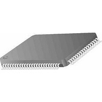
MC68HC11K0CFUE4 Freescale Semiconductor, MC68HC11K0CFUE4 Datasheet - Page 41

MC68HC11K0CFUE4
Manufacturer Part Number
MC68HC11K0CFUE4
Description
MCU 8-BIT 768 RAM 4MHZ 80-QFP
Manufacturer
Freescale Semiconductor
Series
HC11r
Specifications of MC68HC11K0CFUE4
Core Processor
HC11
Core Size
8-Bit
Speed
4MHz
Connectivity
SCI, SPI
Peripherals
POR, PWM, WDT
Number Of I /o
37
Program Memory Type
ROMless
Ram Size
768 x 8
Voltage - Supply (vcc/vdd)
4.5 V ~ 5.5 V
Data Converters
A/D 8x8b
Oscillator Type
Internal
Operating Temperature
-40°C ~ 85°C
Package / Case
80-QFP
Data Bus Width
8 bit
Data Ram Size
768 B
Interface Type
SCI, SPI
Maximum Clock Frequency
4 MHz
Number Of Programmable I/os
37
Number Of Timers
8
Maximum Operating Temperature
+ 85 C
Mounting Style
SMD/SMT
Minimum Operating Temperature
- 40 C
On-chip Adc
8 bit, 8 Channel
Lead Free Status / RoHS Status
Lead free / RoHS Compliant
Eeprom Size
-
Program Memory Size
-
Lead Free Status / Rohs Status
Details
Available stocks
Company
Part Number
Manufacturer
Quantity
Price
Company:
Part Number:
MC68HC11K0CFUE4
Manufacturer:
Freescale Semiconductor
Quantity:
10 000
- Current page: 41 of 290
- Download datasheet (4Mb)
2.10 V
2.11 Port Signals
M68HC11K Family
MOTOROLA
RH
and V
RL
The MODB pin is grounded to select special modes, and has no function
after reset. To select the normal operating modes (single-chip and
expanded) the MODB pin is pulled to a logic high level. Connecting
MODB to a voltage source other than V
battery backup input, V
threshold (about 0.7 volts) below the voltage at V
and part of the reset logic are powered from V
Reset must be driven low before V
until V
to utilize V
significant amount of external circuitry operates from V
shows a suggested circuit employing the V
These pins provide the reference voltage for the analog-to-digital
converter.
The K series contains 62 input/output lines arranged in eight ports, A
through H; all ports are eight bits except port D, which is six bits. The KS
series drops seven lines from port G and four from port H, for a total of
Freescale Semiconductor, Inc.
For More Information On This Product,
DD
has been restored to a valid level. The extra hardware required
STBY
Go to: www.freescale.com
4.8 V
NICD
may be justified in certain applications where a
Figure 2-9. MODB/V
V
Pin Description
DD
+
STBY.
V
V
BATT
DD
MAX
690
When V
V Out
DD
DD
STBY
is removed and must remain low
4.7 K
DD
drops more than one MOS
enables it to function as a
STBY
Connection
STBY
TO MODB/ V
OF M68HC11
pin.
STBY
rather than V
, the MCU’s RAM
DD
STBY
.
Figure 2-9
Pin Description
Technical Data
VRH and VRL
DD
.
41
Related parts for MC68HC11K0CFUE4
Image
Part Number
Description
Manufacturer
Datasheet
Request
R

Part Number:
Description:
MC68HC11 EEPROM Programming from a Personal Computer
Manufacturer:
Motorola / Freescale Semiconductor
Part Number:
Description:
Manufacturer:
Freescale Semiconductor, Inc
Datasheet:
Part Number:
Description:
Manufacturer:
Freescale Semiconductor, Inc
Datasheet:
Part Number:
Description:
Manufacturer:
Freescale Semiconductor, Inc
Datasheet:
Part Number:
Description:
Manufacturer:
Freescale Semiconductor, Inc
Datasheet:
Part Number:
Description:
Manufacturer:
Freescale Semiconductor, Inc
Datasheet:
Part Number:
Description:
Manufacturer:
Freescale Semiconductor, Inc
Datasheet:
Part Number:
Description:
Manufacturer:
Freescale Semiconductor, Inc
Datasheet:
Part Number:
Description:
Manufacturer:
Freescale Semiconductor, Inc
Datasheet:
Part Number:
Description:
Manufacturer:
Freescale Semiconductor, Inc
Datasheet:
Part Number:
Description:
Manufacturer:
Freescale Semiconductor, Inc
Datasheet:
Part Number:
Description:
Manufacturer:
Freescale Semiconductor, Inc
Datasheet:
Part Number:
Description:
Manufacturer:
Freescale Semiconductor, Inc
Datasheet:
Part Number:
Description:
Manufacturer:
Freescale Semiconductor, Inc
Datasheet:
Part Number:
Description:
Manufacturer:
Freescale Semiconductor, Inc
Datasheet:


