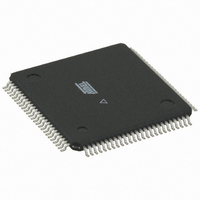
AT91R40807-33AI Atmel, AT91R40807-33AI Datasheet - Page 10

AT91R40807-33AI
Manufacturer Part Number
AT91R40807-33AI
Description
IC ARM7 MCU 176 TQFP
Manufacturer
Atmel
Series
AT91SAMr
Datasheets
1.AT91R40807-33AC.pdf
(19 pages)
2.AT91R40807-33AC.pdf
(20 pages)
3.AT91R40807-33AI.pdf
(153 pages)
Specifications of AT91R40807-33AI
Core Processor
ARM7
Core Size
16/32-Bit
Speed
33MHz
Connectivity
EBI/EMI, UART/USART
Peripherals
WDT
Number Of I /o
32
Program Memory Type
ROMless
Ram Size
136K x 8
Voltage - Supply (vcc/vdd)
1.8 V ~ 3.6 V
Oscillator Type
External
Operating Temperature
-40°C ~ 85°C
Package / Case
100-TQFP, 100-VQFP
Lead Free Status / RoHS Status
Contains lead / RoHS non-compliant
Eeprom Size
-
Program Memory Size
-
Data Converters
-
Available stocks
Company
Part Number
Manufacturer
Quantity
Price
Company:
Part Number:
AT91R40807-33AI
Manufacturer:
ATMEL
Quantity:
1 831
ROM Emulation
Boot Mode Select
Remap Command
Abort Control
10
AT91X40 Series
The AT91R40807 provides an ideal means of emulating the ROM version
AT91M40807. The secondary SRAM bank of the AT91R40807 is mapped to the same
address as the ROM of the AT91M40807. It is write-protected after a reset; writing 0x1
in the Memory Mode Register of the Special Function Module can disable this
protection.
At system power-up, the code is downloaded from an external non-volatile memory or
through a debugger to the on-chip secondary SRAM bank of the AT91R40807. After the
secondary SRAM bank write-protection is enabled, the application is in the same envi-
ronment as though it were running on an AT91M40807.
The ARM reset vector is at address 0x0. After the NRST line is released, the
ARM7TDMI executes the instruction stored at this address. This means that this
address must be mapped in non-volatile memory after the reset.
The input level on the BMS pin during the last 10 clock cycles before the rising edge of
the NRST selects the type of boot memory. The Boot Mode depends on BMS and
whether or not the AT91X40 Series Microcontroller has on-chip ROM or extended
SRAM (see Table 3).
The AT91R40807 supports boot in on-chip extended SRAM, for the purpose of emulat-
ing ROM versions. In this case, the microcontroller must first boot from external non-
volatile memory, and ensure that a valid program is downloaded in the on-chip extended
SRAM. Then, the NRST must be reasserted by external circuitry after the level on the
pin BMS is changed.
The pin BMS is multiplexed with the I/O line P24 that can be programmed after reset like
any standard PIO line.
Table 3. Boot Mode Select
The ARM vectors (Reset, Abort, Data Abort, Prefetch Abort, Undefined Instruction,
Interrupt, Fast Interrupt) are mapped from address 0x0 to address 0x20. In order to
allow these vectors to be redefined dynamically by the software, the AT91X40 Series
Microcontrollers use a remap command that enables switching between the boot mem-
ory and the internal primary SRAM bank addresses. The remap command is accessible
through the EBI User Interface, by writing one in RCB of EBI_RCR (Remap Control
Register). Performing a remap command is mandatory if access to the other external
devices (connected to chip selects 1 to 7) is required. The remap operation can only be
changed back by an internal reset or an NRST assertion.
The abort signal providing a Data Abort or a Prefetch Abort exception to the ARM7TDMI
is asserted in the following cases:
•
•
BMS
1
0
When accessing an undefined address in the EBI address space
When writing to a write-protected internal memory area on the AT91R40807
Product
AT91M40800
AT91R40807
AT91M40807
AT91R40008
All
Boot Memory
External 8-bit memory on NCS0
Internal 32-bit extended SRAM
Internal 32-bit ROM
External 8-bit memory on NCS0
External 16-bit memory on NCS0
1354D–ATARM–08/02


