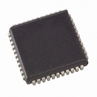
AT89LS8252-12JC Atmel, AT89LS8252-12JC Datasheet - Page 9

AT89LS8252-12JC
Manufacturer Part Number
AT89LS8252-12JC
Description
IC MICRO CTRL 12MHZ 44PLCC
Manufacturer
Atmel
Series
89LSr
Datasheet
1.AT89LS8252-12AC.pdf
(35 pages)
Specifications of AT89LS8252-12JC
Core Processor
8051
Core Size
8-Bit
Speed
12MHz
Connectivity
SPI, UART/USART
Peripherals
POR, WDT
Number Of I /o
32
Program Memory Size
8KB (8K x 8)
Program Memory Type
FLASH
Eeprom Size
2K x 8
Ram Size
256 x 8
Voltage - Supply (vcc/vdd)
2.7 V ~ 6 V
Oscillator Type
Internal
Operating Temperature
0°C ~ 70°C
Package / Case
44-PLCC
Lead Free Status / RoHS Status
Contains lead / RoHS non-compliant
Data Converters
-
Other names
AT89LS825212JC
Available stocks
Company
Part Number
Manufacturer
Quantity
Price
Table 6. SPDR—SPI Data Register
Data Memory—EEPROM and RAM
The AT89LS8252 implements 2K bytes of on-chip
EEPROM for data storage and 256 bytes of RAM. The
upper 128 bytes of RAM occupy a parallel space to the
Special Function Registers. That means the upper 128
bytes have the same addresses as the SFR space but are
physically separate from SFR space.
When an instruction accesses an internal location above
address 7FH, the address mode used in the instruction
specifies whether the CPU accesses the upper 128 bytes
of RAM or the SFR space. Instructions that use direct
addressing access SFR space.
For example, the following direct addressing instruction
accesses the SFR at location 0A0H (which is P2).
Instructions that use indirect addressing access the upper
128 bytes of RAM. For example, the following indirect
addressing instruction, where R0 contains 0A0H, accesses
the data byte at address 0A0H, rather than P2 (whose
address is 0A0H).
Note that stack operations are examples of indirect
addressing, so the upper 128 bytes of data RAM are avail-
able as stack space.
The on-chip EEPROM data memory is selected by setting
the EEMEN bit in the WMCON register at SFR address
location 96H. The EEPROM address range is from 000H to
7FFH. The MOVX instructions are used to access the
EEPROM. To access off-chip data memory with the MOVX
instructions, the EEMEN bit needs to be set to “0”.
The EEMWE bit in the WMCON register needs to be set to
“1” before any byte location in the EEPROM can be written.
User software should reset EEMWE bit to “0” if no further
EEPROM write is required. EEPROM write cycles in the
serial programming mode are self-timed and typically take
2.5 ms. The progress of EEPROM write can be monitored
by reading the RDY/BSY bit (read-only) in SFR WMCON.
RDY/BSY = 0 means programming is still in progress and
RDY/BSY = 1 means EEPROM write cycle is completed
and another write cycle can be initiated.
0850C–MICRO–3/06
SPDR Address = 86HReset Value = unchanged
Bit
MOV 0A0H, #data
MOV @R0, #data
SPD7
7
SPD6
6
SPD5
5
SPD4
4
SPD3
3
In addition, during EEPROM programming, an attempted
read from the EEPROM will fetch the byte being written
with the MSB complemented. Once the write cycle is com-
pleted, true data are valid at all bit locations.
Programmable Watchdog Timer
The programmable Watchdog Timer (WDT) operates from
an independent oscillator. The prescaler bits, PS0, PS1
and PS2 in SFR WMCON are used to set the period of the
Watchdog Timer from 16 ms to 2048 ms. The available
timer periods are shown in the following table and the
actual timer periods (at V
nominal.
The WDT is disabled by Power-on Reset and during Power
Down. It is enabled by setting the WDTEN bit in SFR
WMCON (address = 96H). The WDT is reset by setting the
WDTRST bit in WMCON. When the WDT times out without
being reset or disabled, an internal RST pulse is generated
to reset the CPU.
Table 7. Watchdog Timer Period Selection
PS2
0
0
0
0
1
1
1
1
WDT Prescaler Bits
SPD2
2
PS1
0
0
1
1
0
0
1
1
SPD1
1
CC
= 5V) are within ±30% of the
PS0
0
1
0
1
0
1
0
1
AT89LS8252
SPD0
0
Period (nominal)
16 ms
32 ms
64 ms
128 ms
256 ms
512 ms
1024 ms
2048 ms
9


