ATMEGA323L-4AI Atmel, ATMEGA323L-4AI Datasheet
ATMEGA323L-4AI
Specifications of ATMEGA323L-4AI


Related parts for ATMEGA323L-4AI


ATMEGA323L-4AI Summary of contents
Page 1
... I/O and Packages – 32 Programmable I/O Lines – 40-pin PDIP and 44-lead TQFP • Operating Voltages – 2.7 - 5.5V (ATmega323L) – 4.0 - 5.5V (ATmega323) • Speed Grades – MHz (ATmega323L) – MHz (ATmega323) ® 8-bit Microcontroller 8-bit Microcontroller with 32K Bytes of In-System Programmable ...
Page 2
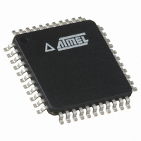
Pin Configurations ATmega323(L) 2 PDIP (XCK/T0) PB0 1 40 (T1) PB1 2 39 (INT2/AIN0) PB2 3 38 (OC0/AIN1) PB3 4 37 (SS) PB4 5 36 (MOSI) PB5 6 35 (MISO) PB6 7 34 (SCK) PB7 8 33 RESET 9 32 ...
Page 3
Overview The ATmega323 is a low-power CMOS 8-bit microcontroller based on the AVR enhanced RISC architecture. By executing powerful instructions in a single clock cycle, the ATmega323 achieves throughputs approaching 1 MIPS per MHz allowing the sys- tem designer to ...
Page 4
... Application Flash memory. By com- bining an 8-bit RISC CPU with In-System Programmable Flash on a monolithic chip, the Atmel ATmega323 is a powerful microcontroller that provides a highly flexible and cost effective solution to many embedded control applications. The ATmega323 AVR is supported with a full suite of program and system development tools including: C compilers, macro assemblers, program debugger/simulators, In-Cir- cuit Emulators, and evaluation kits ...
Page 5
Port B (PB7..PB0) Port 8-bit bi-directional I/O port with internal pull-up resistors (selected for each bit). The Port B output buffers can sink 20 mA. As inputs, Port B pins that are externally pulled low will source ...
Page 6
Clock Options Internal RC Oscillator Crystal Oscillator ATmega323(L) 6 The device has the following clock source options, selectable by Flash Fuse bits as shown: Table 1. Device Clocking Options Select Device Clocking Option External Crystal/Ceramic Resonator External Low-frequency Crystal External ...
Page 7
External Clock To drive the device from an external clock source, XTAL1 should be driven as shown in Figure 3. Figure 3. External Clock Drive Configuration External RC Oscillator For timing insensitive applications, the external RC configuration shown in Figure ...
Page 8
Architectural Overview ATmega323(L) 8 The fast-access Register File concept contains 32 x 8-bit general purpose working reg- isters with a single clock cycle access time. This means that during one single clock cycle, one Arithmetic Logic Unit (ALU) operation is ...
Page 9
Figure 5. The ATmega323 AVR Enhanced RISC Architecture The AVR uses a Harvard architecture concept – with separate memories and buses for Program and Data. The Program memory is executed with a single level pipelining. While one instruction is being ...
Page 10
ATmega323(L) 10 The 2K bytes data SRAM can be easily accessed through the five different addressing modes supported in the AVR architecture. The memory spaces in the AVR architecture are all linear and regular memory maps. A flexible interrupt module ...
Page 11
The General Purpose Figure 7 shows the structure of the 32 general purpose working registers in the CPU. Register File Figure 7. AVR CPU General Purpose Working Registers Most register operating instructions in the instruction set have direct access to ...
Page 12
The ALU Arithmetic – Logic Unit The In-System Reprogrammable Flash Program Memory The SRAM Data Memory ATmega323(L) 12 The high-performance AVR ALU operates in direct connection with all the 32 general purpose working registers. Within a single clock cycle, ALU ...
Page 13
Figure 9. SRAM Organization The Program and Data The ATmega323 AVR Enhanced RISC microcontroller supports powerful and efficient addressing modes for access to the Program memory (Flash) and Data memory Addressing Modes (SRAM, Register File, and I/O Memory). This section ...
Page 14
Register Direct, Two Registers Rd and Rr I/O Direct Data Direct ATmega323(L) 14 Figure 11. Direct Register Addressing, Two Registers Operands are contained in register r (Rr) and d (Rd). The result is stored in register d (Rd). Figure 12. ...
Page 15
Data Indirect with Figure 14. Data Indirect with Displacement Displacement Operand address is the result of the Y- or Z-register contents added to the address con- tained in 6 bits of the instruction word. Data Indirect Figure 15. Data Indirect ...
Page 16
Data Indirect with Post- increment Constant Addressing Using the LPM and SPM Instructions Indirect Program Addressing, IJMP and ICALL ATmega323(L) 16 Figure 17. Data Indirect Addressing With Post-increment REGISTER The X-, Y-, or the ...
Page 17
Relative Program Addressing, Figure 20. Relative Program Memory Addressing RJMP and RCALL Program execution continues at address The relative address k is from – 2048 to 2047. The EEPROM Data The ATmega323 contains 1K bytes ...
Page 18
I/O Memory ATmega323(L) 18 Figure 22. Single Cycle ALU Operation T1 System Clock Ø Total Execution Time Register Operands Fetch ALU Operation Execute Result Write Back The internal data SRAM access is performed in two System Clock cycles as described ...
Page 19
Table 2. ATmega323 I/O Space (Continued) 1457G–AVR–09/03 I/O Address (SRAM Address) Name Function $33 ($53) TCCR0 Timer/Counter0 Control Register $32 ($52) TCNT0 Timer/Counter0 (8-bit) OSCCAL Oscillator Calibration Register (1) $31 ($51) OCDR On-chip Debug Register $30 ($50) SFIOR Special Function ...
Page 20
ATmega323(L) 20 Table 2. ATmega323 I/O Space (Continued) I/O Address (SRAM Address) Name $12 ($32) PORTD $11 ($31) DDRD $10 ($30) PIND $0F ($2F) SPDR $0E ($2E) SPSR $0D ($2D) SPCR $0C ($2C) UDR $0B ($2B) UCSRA $0A ($2A) UCSRB ...
Page 21
The Status Register – SREG The AVR Status Register • Bit 7 – I: Global Interrupt Enable The Global Interrupt Enable bit must be set (one) for the interrupts to be enabled. The individual Interrupt Enable control is then performed ...
Page 22
The Stack Pointer SP – Reset and Interrupt Handling ATmega323(L) 22 The ATmega323 Stack Pointer is implemented as two 8-bit registers in the I/O space locations $3E ($5E) and $3D ($5D). As the ATmega323 Data memory has $860 loca- tions, ...
Page 23
Table 3. Reset and Interrupt Vectors (Continued) Notes: Table 4 shows Reset and Interrupt Vectors placement for the various combinations of BOOTRST and IVSEL settings. Table 4. Reset and Interrupt Vectors Placement Note: The most typical and general program setup ...
Page 24
ATmega323(L) 24 $018 jmp SPI_STC; $01a jmp USART_RXC $01c jmp USART_UDRE ; UDR Empty Handler $01e jmp USART_TXC $020 jmp ADC $022 jmp EE_RDY $024 jmp ANA_COMP $026 jmp TWSI Handler ; $028 MAIN: ldi r16,high(RAMEND); Main program start $029 ...
Page 25
When the BOOTRST Fuse is programmed, the boot section size set to 4K bytes and the IVSEL bit in the GICR Register is set before any interrupts are enabled, the most typical and general program setup for the Reset and ...
Page 26
ATmega323(L) 26 Figure 24. Reset Logic Power- Reset Circuit Brown-out BODEN Reset Circuit BODLEVEL 100-500k SPIKE Reset Circuit RESET FILTER JTAG Reset Watchdog Register Timer On-chip RC Oscillator Clock Generator CKSEL[3:0] (1) Table 5. Reset Characteristics Symbol Parameter ...
Page 27
Table 6. Reset Delay Selections Notes: 1457G–AVR–09/03 (1) Start-up Time 2.7V, BODLEVEL (2) CKSEL Unprogrammed 0000 4 (4) 0001 30 µ (6) 0010 0011 4.2 ...
Page 28
Power-on Reset ATmega323(L) 28 Table 6 shows the start-up times from Reset. When the CPU wakes up from Power- down or Power-save, only the clock counting part of the start-up time is used. The Watchdog Oscillator is used for timing ...
Page 29
Figure 26. MCU Start-up, RESET Extended Externally External Reset An External Reset is generated by a low level on the RESET pin. Reset pulses longer than 500 ns will generate a reset, even if the clock is not running. Shorter ...
Page 30
Watchdog Reset MCU Control and Status Register – MCUCSR ATmega323(L) 30 Figure 28. Brown-out Reset During Operation RESET TIME-OUT INTERNAL RESET The hysteresis BOT BOT+ When the Watchdog times out, it ...
Page 31
Bit 6 – ISC2: Interrupt Sense Control 2 The asynchronous external interrupt 2 is activated by the external pin INT2 if the SREG I-flag and the corresponding interrupt mask in the GICR are set. If ISC2 is cleared (zero), ...
Page 32
Voltage Reference Enable Signals and Start-up Time Interrupt Handling Interrupt Response Time ATmega323(L) 32 The voltage reference has a start-up time that may influence the way it should be used. The maximum start-up time is TBD. To save power, the ...
Page 33
The General Interrupt Control l Register – GICR • Bit 7 – INT1: External Interrupt Request 1 Enable When the INT1 bit is set (one) and the I-bit in the Status Register (SREG) is set (one), the external pin interrupt ...
Page 34
The General Interrupt Flag Register – GIFR The Timer/Counter Interrupt Mask Register – TIMSK ATmega323(L) 34 Note: If Boot Lock bits BLB02 or BLB12 are set, changing the Interrupt Vector table will change from what part of the Program memory ...
Page 35
Bit 6 – TOIE2: Timer/Counter2 Overflow Interrupt Enable When the TOIE2 bit is set (one) and the I-bit in the Status Register is set (one), the Timer/Counter2 Overflow interrupt is enabled. The corresponding interrupt is executed if an overflow ...
Page 36
The Timer/Counter Interrupt Flag Register – TIFR ATmega323(L) 36 Bit $38 ($58) OCF2 TOV2 ICF1 Read/Write R/W R/W R/W Initial Value • Bit 7 – OCF2: Output Compare Flag 2 The OCF2 bit is ...
Page 37
Bit 2 – TOV1: Timer/Counter1 Overflow Flag The TOV1 is set (one) when an overflow occurs in Timer/Counter1. TOV1 is cleared by hardware when executing the corresponding interrupt handling vector. Alternatively, TOV1 is cleared by writing a logic one ...
Page 38
ATmega323(L) 38 • Bits 6..4 – SM2..0: Sleep Mode Select Bits 2, 1 and 0 These bits select between the six available sleep modes as shown in Table 8. Table 8. Sleep Mode Select SM2 SM1 SM0 ...
Page 39
Table 10. Interrupt 0 Sense Control Sleep Modes To enter any of the six sleep modes, the SE bit in MCUCR must be set (one) and a SLEEP instruction must be executed. The SM2, SM1, and SM0 bits in the ...
Page 40
Power-down Mode Power-save Mode Standby Mode Extended Standby Mode ATmega323(L) 40 When the SM2..0 bits are 010, the SLEEP instruction makes the MCU enter Power- down mode. In this mode, the external Oscillator is stopped, while the external inter- rupts, ...
Page 41
Calibrated Internal The calibrated internal Oscillator provides a fixed 1.0 MHz (nominal) clock at 5V and 25 C. This clock may be used as the system clock. See the section “Clock Options” Oscillator page 6 for information on ...
Page 42
ATmega323(L) 42 • Bit 1 – PSR2: Prescaler Reset Timer/Counter2 When this bit is set (one) the Timer/Counter2 prescaler will be reset. The bit will be cleared by hardware after the operation is performed. Writing a zero to this bit ...
Page 43
Timer/Counters The ATmega323 provides three general purpose Timer/Counters – two 8-bit T/Cs and one 16-bit T/C. Timer/Counter2 can optionally be asynchronously clocked from an exter- nal Oscillator. This Oscillator is optimized for use with a 32.768 kHz watch crystal, enabling ...
Page 44
ATmega323(L) 44 Figure 31. Prescaler for Timer/Counter2 CK PCK2 Clear XTAL1 AS2 PSR2 CS20 CS21 CS22 The clock source for Timer/Counter2 is named PCK2. PCK2 is by default connected to the main system clock CK. By setting the AS2 bit ...
Page 45
Timers/Counters Figure 32 shows the block diagram for Timer/Counter0. Figure 33 shows the block dia- gram for Timer/Counter2. Timer/Counter0 and Timer/Counter2 Figure 32. Timer/Counter0 Block Diagram 1457G–AVR–09/03 T/C0 OVER- T/C0 COMPARE FLOW IRQ MATCH IRQ TIMER INT. MASK TIMER ...
Page 46
ATmega323(L) 46 Figure 33. Timer/Counter2 Block Diagram T/C2 OVER- FLOW IRQ 8-BIT DATA BUS 8-BIT ASYNCH T/C2 DATA BUS TIMER INT. MASK REGISTER (TIMSK T/C CLEAR TIMER/COUNTER2 T/C CLK SOURCE (TCNT2) UP/DOWN 7 0 8-BIT COMPARATOR 7 0 ...
Page 47
Timer/Counter0 and 2 can also be used as 8-bit Pulse Width Modulators. In this mode, the Timer/Counter and the Output Compare Register serve as a glitch-free, stand-alone PWM with centered pulses. Refer to page 49 for a detailed description on ...
Page 48
ATmega323(L) 48 • Bit 3 – CTC0/CTC2: Clear Timer/Counter on Compare Match When the CTC0 or CTC2 control bit is set (one), Timer/Counter0 or Timer/Counter2 is reset to $00 in the CPU clock cycle following a Compare Match. If the ...
Page 49
The Stop condition provides a Timer Enable/Disable function. The prescaled modes are scaled directly from the CK Oscillator clock for Timer/Counter0 and PCK2 for Timer/Counter2. If the external pin modes are used for Timer/Counter0, transitions on PB0(T0) will clock the ...
Page 50
PWM Modes (Up/Down and Overflow) ATmega323(L) 50 The two different PWM modes are selected by the CTC0 or CTC2 bit in the Timer/Counter Control Registers –TCCR0 or TCCR2 respectively. If CTC0/CTC2 is cleared and PWM mode is selected, the Timer/Counter ...
Page 51
Figure 34. Effects of Unsynchronized OCR Latching in Up/Down Mode Figure 35. Effects of Unsynchronized OCR Latching in Overflow Mode Note: During the time between the write and the latch operation, a read from the Output Com- pare Registers will ...
Page 52
Asynchronous Status Register – ASSR ATmega323(L) 52 Table 16. PWM Outputs OCRn = $00 or $FF COMn1 COMn0 Note overflow PWM mode, the table above ...
Page 53
If a write is performed to any of the three Timer/Counter2 Registers while its Update Busy Flag is set (one), the updated value might get corrupted and cause an uninten- tional interrupt to occur. The mechanisms for reading TCNT2, OCR2, ...
Page 54
Timer/Counter1 ATmega323(L) 54 Power-up Reset or wake-up from Power-down or Standby mode, the user should be aware of the fact that this Oscillator might take as long as one second to stabilize. The user is advised to wait for ...
Page 55
Register B – TCCR1B” on page 57. The different Status Flags (Overflow, Compare Match, and Capture Event) are found in the Timer/Counter Interrupt Flag Register – TIFR. Control signals are found in the Timer/Counter1 Control Registers – TCCR1A and TCCR1B. ...
Page 56
Timer/Counter1 Control Register A – TCCR1A ATmega323(L) 56 Bit $2F ($4F) COM1A1 COM1A0 COM1B1 Read/Write R/W R/W R/W Initial Value • Bits 7, 6 – COM1A1, COM1A0: Compare Output Mode1A, Bits 1 and 0 ...
Page 57
Compare Match had occurred, but no interrupt is generated. The corresponding I/O pin must be set as an output pin for the FOC1B bit to have effect on the pin. The FOC1B bit will always be read as zero. ...
Page 58
Timer/Counter1 – TCNT1H and TCNT1L ATmega323(L) 58 When the prescaler is set to divide by 8, the timer will count like this: ... | C-1, C-1, C-1, C-1, C-1, C-1, C-1, C ...
Page 59
TCNT1 Timer/Counter1 Write When the CPU writes to the High Byte TCNT1H, the written data is placed in the TEMP Register. Next, when the CPU writes the Low Byte TCNT1L, this byte of data is com- bined with the byte ...
Page 60
Timer/Counter1 Input Capture Register – ICR1H and ICR1L Timer/Counter1 In PWM Mode ATmega323(L) 60 The TEMP Register is also used when accessing TCNT1 and ICR1. If the main program and also interrupt routines perform access to registers using TEMP, interrupts ...
Page 61
Table 20. Timer TOP Values and PWM Frequency As shown in Table 20, the PWM operates at either bits resolution. Note the unused bits in OCR1A, OCR1B, and TCNT1 will automatically be written to zero by ...
Page 62
ATmega323(L) 62 Figure 38. Effects of Unsynchronized OCR1 Latching. Synchronized OC1x Latch Unsynchronized OC1x Latch Note Figure 39. Effects of Unsynchronized OCR1 Latching in Overflow Mode Synchronized OC1x Latch Unsynchronized OC1x Latch Note ...
Page 63
Table 23. PWM Outputs OCR1X = $0000 or TOP In overflow PWM mode, the table above is only valid for OCR1X = TOP. In PWM mode, the Timer Overflow Flag1, TOV1, is set when the counter advances from $0000. In ...
Page 64
Watchdog Timer The Watchdog Timer Control Register – WDTCR ATmega323(L) 64 The Watchdog Timer is clocked from a separate On-chip Oscillator which runs at 1 Mhz. This is the typical value 5V. See characterization data for typical ...
Page 65
In the same operation, write a logical one to WDTOE and WDE. A logical one 2. Within the next four clock cycles, write a logical 0 to WDE. This disables the • Bits 2..0 – WDP2, WDP1, WDP0: Watchdog ...
Page 66
EEPROM Read/Write Access The EEPROM Address Register – EEARH and EEARL The EEPROM Data Register – EEDR ATmega323(L) 66 The EEPROM Access Registers are accessible in the I/O space. The write access time is in the range of 1.9 - ...
Page 67
The EEPROM Control Register – EECR • Bits 7..4 – Res: Reserved Bits These bits are reserved bits in the ATmega323 and will always read as zero. • Bit 3 – EERIE: EEPROM Ready Interrupt Enable When the I bit ...
Page 68
Preventing EEPROM Corruption ATmega323(L) 68 The user should poll the EEWE bit before starting the read operation write operation is in progress not possible to set the EERE bit, nor to change the EEAR Register. The ...
Page 69
Serial Peripheral The Serial Peripheral Interface (SPI) allows high-speed synchronous data transfer between the ATmega323 and peripheral devices or between several AVR devices. The Interface – SPI ATmega323 SPI includes the following features: • • • • • • • ...
Page 70
SS Pin Functionality ATmega323(L) 70 Figure 42. SPI Master-Slave Interconnection MSB MASTER LSB 8 BIT SHIFT REGISTER SPI CLOCK GENERATOR The system is single buffered in the transmit direction and double buffered in the receive direction. This means that bytes ...
Page 71
SS pin is driven high. If the SS pin is driven high during a transmission, the SPI will stop sending and receiving immediately and both data received and data sent must be considered as lost. Data Modes There ...
Page 72
The SPI Status Register – SPSR ATmega323(L) 72 • Bit 5 – DORD: Data Order When the DORD bit is set (one), the LSB of the data word is transmitted first. When the DORD bit is cleared (zero), the MSB ...
Page 73
Bit 6 – WCOL: Write COLlision Flag The WCOL bit is set if the SPI Data Register (SPDR) is written during a data transfer. The WCOL bit (and the SPIF bit) are cleared (zero) by first reading the SPI ...
Page 74
USART Overview ATmega323(L) 74 The Universal Synchronous and Asynchronous serial Receiver and Transmitter (USART highly flexible serial communication device. The main features are: • Full Duplex Operation (Independent Serial Receive and Transmit Registers) • Asynchronous or Synchronous Operation ...
Page 75
XCK (transfer clock) pin is only used by synchronous transfer mode. The Transmitter consists of a single write buffer, a serial Shift Register, Parity Generator and control logic for handling different serial frame formats. The write buffer allows a continuous ...
Page 76
Clock Generation Internal Clock Generation – The Baud Rate Generator ATmega323(L) 76 The Clock Generation Logic generates the base clock for the Transmitter and Receiver. The USART supports four modes of clock operation: Normal asynchronous, Double Speed asynchronous, Master synchronous ...
Page 77
Table 29 contains equations for calculating the baud rate (in bits per second) and for calculating the UBRR value for each mode of operation using an internally generated clock source. Table 29. Equations for Calculating Baud Rate Register Setting Note: ...
Page 78
Frame Formats ATmega323(L) 78 Figure 47. Synchronous Mode XCK Timing UCPOL = 0 XCK RxD / TxD UCPOL = 1 XCK RxD / TxD The UCPOL bit UCRSC selects which XCK clock edge is used for data sampling and which ...
Page 79
The frame format used by the USART is set by the UCSZ2:0, UPM1:0 and USBS bits in UCSRB and UCSRC. The Receiver and Transmitter uses the same setting. Note that changing the setting of any of these bits will corrupt ...
Page 80
ATmega323(L) 80 (1) Assembly Code Example USART_Init: ; Set baud rate out UBRRH, r17 out UBRRL, r16 ; Enable Receiver and Transmitter ldi r16, (1<<RXEN)|(1<<TXEN) out UCSRB,r16 ; Set frame format: 8data, 2stop bit ldi r16, (1<<URSEL)|(1<<USBS)|(3<<UCSZ0) out UCSRC,r16 ret ...
Page 81
Data Transmission – The The USART Transmitter is enabled by setting the Transmit Enable (TXEN) bit in the UCSRB Register. When the Transmitter is enabled, the normal port operation of the USART Transmitter TxD pin is overridden by the USART ...
Page 82
Sending Frames with 9 Data Bit Transmitter Flags and Interrupts ATmega323( 9-bit characters are used (UCSZ = 7), the ninth bit must be written to the TXB8 bit in UCSRB before the Low Byte of the character written ...
Page 83
Empty Interrupt, otherwise a new interrupt will occur once the interrupt routine terminates. The Transmit Complete (TXC) Flag bit is set one when the entire frame in the Transmit Shift Register has been shifted out and there are no new ...
Page 84
Data Reception – The USART Receiver Receiving Frames with Data Bits ATmega323(L) 84 The USART Receiver is enabled by setting the Receive Enable (RXEN) bit in the UCSRB Register. When the Receiver is enabled, the normal pin ...
Page 85
Receiving Frames with 9 Data If 9-bit characters are used (UCSZ=7) the ninth bit must be read from the RXB8 bit in Bits UCSRB before reading the low bits from the UDR. This rule applies to the FE, DOR, and ...
Page 86
Receive Compete Flag and Interrupt Receiver Error Flags ATmega323(L) 86 The receive function example reads all the I/O Registers into the Register File before any computation is done. This gives an optimal receive buffer utilization since the buffer location read ...
Page 87
Parity Checker The parity checker is active when the high USART Parity Mode (UPM1) bit is set. Type of parity check to be performed (odd or even) is selected by the UPM0 bit. When enabled, the parity checker calculates the ...
Page 88
Asynchronous Data Reception Asynchronous Clock Recovery Asynchronous Data Recovery ATmega323(L) 88 The USART includes a clock recovery and a data recovery unit for handling asynchro- nous data reception. The clock recovery logic is used for synchronizing the internally generated baud ...
Page 89
The decision of the logic level of the received bit is taken by doing a majority voting of the logic value to the three samples in the center of the received bit. The center samples are emphasized on the figure ...
Page 90
ATmega323( the ratio of the slowest incoming data rate that can be accepted in relation to the slow Receiver baud rate the ratio of the fastest incoming data rate that can be fast accepted in ...
Page 91
Multi-processor Setting the Multi-Processor Communication mode (MPCM) bit in UCSRA enables a fil- tering function of incoming frames received by the USART Receiver. Frames that do not Communication Mode contain address information will be ignored and not put into the ...
Page 92
Accessing UBRRH/UCSRC Registers Write Access ATmega323(L) 92 The UBRRH Register shares the same I/O location as the UCSRC Register. Therefore some special consideration must be taken when accessing this I/O location. When doing a write access of this I/O location, ...
Page 93
Read Access Doing a read access to the UBRRH or the UCSRC Register is a more complex opera- tion. However, in most applications rarely necessary to read any of these registers. The read access is controlled by a ...
Page 94
USART Register Description USART I/O Data Register – UDR USART Control and Status Register A – UCSRA ATmega323(L) 94 Bit $0C ($2C) Read $0C ($2C) Write Read/Write R/W R/W R/W Initial Value The USART ...
Page 95
Bit 5 – UDRE: USART Data Register Empty The UDRE Flag indicates if the transmit buffer (UDR) is ready to receive new data. If UDRE is one the buffer is empty and therefore ready be written. The UDRE Flag ...
Page 96
USART Control and Status Register B – UCSRB ATmega323(L) 96 Bit $0A ($2A) RXCIE TXCIE UDRIE Read/Write R/W R/W R/W Initial Value • Bit 7 – RXCIE: RX Complete Interrupt Enable Setting this bit ...
Page 97
USART Control and Status Register C – UCSRC The UCSRC Register shares the same I/O location as the UBRRH Register. See the “Accessing UBRRH/UCSRC Registers” on page 92 section which describes how to access this register. • Bit 7 – ...
Page 98
USART Baud Rate Registers – UBRRL and UBRRHs ATmega323(L) 98 • Bit 2:1 – UCSZ1:0: Character Size The UCSZ1:0 bits combined with the UCSZ2 bit in UCSRB sets the number of data bits (character size frame the Receiver ...
Page 99
Bit 11:0 – UBRR11:0: USART Baud Rate Register This is a 12-bit register which contains the USART baud rate. The UBRRH contains the four most significant bits, and the UBRRL contains the eight least significant bits of the USART ...
Page 100
ATmega323(L) 100 Table 36. Examples of UBRR Settings for Commonly Used Oscillator Frequencies – (Continued) UBRR = 0, Error = 0.0% 14.4K 8 -3.5% 16 19.2K 6 -7.0% 12 28.8K 3 8.5% 8 38.4K 2 8.5% 6 57.6K 1 8.5% ...
Page 101
Table 36. Examples of UBRR Settings for Commonly Used Oscillator Frequencies – UBRR = 0, Error = 0.0% 1457G–AVR–09/03 (Continued) 19.2K 25 0.2% 51 28.8K 16 2.1% 34 38.4K 12 0.2% 25 57.6K 8 -3.5% 16 76.8K 6 -7.0% 12 ...
Page 102
Two-wire Serial Interface (Byte Oriented) ATmega323(L) 102 The Two-wire Serial Interface supports bi-directional serial communication designed primarily for simple but efficient integrated circuit (IC) control. The system is comprised of two lines, SCL (Serial Clock) and SDA (Serial ...
Page 103
Figure 54. Block diagram of the Two-wire Serial Interface The CPU interfaces with the Two-wire Serial Interface via the following five I/O Regis- ters: the Two-wire Serial Interface Bit Rate Register (TWBR), the Two-wire Serial Interface Control Register (TWCR), the ...
Page 104
The Two-wire Serial Interface Bit Rate Register – TWBR The Two-wire Serial Interface Control Register – TWCR ATmega323(L) 104 Bit $00 ($20) TWBR7 TWBR6 TWBR5 Read/Write R/W R/W R/W Initial Value • Bits 7..0 ...
Page 105
By setting the TWEA bit low, the device can be virtually disconnected from the Two-wire Serial Bus temporarily. Address recognition can then be resumed by setting the TWEA bit again. • Bit 5 – TWSTA: Two-wire Serial Bus START Condition ...
Page 106
The Two-wire Serial Interface Status Register – TWSR The Two-wire Serial Interface Data Register – TWDR ATmega323(L) 106 Bit $01 ($21) TWS7 TWS6 TWS5 Read/Write Initial Value • Bits 7..3 – ...
Page 107
The Two-wire Serial Interface (Slave) Address Register – TWAR • Bits 7..1 – TWA: Two-wire Serial Interface (Slave) Address Register These seven bits constitute the slave address of the Two-wire Serial Bus unit. • Bit 0 – TWGCE: Two-wire Serial ...
Page 108
Master Transmitter Mode Master Receiver Mode ATmega323(L) 108 When the Two-wire Serial Interface Interrupt Flag is set, the status code in TWSR is used to determine the appropriate software action. For each status code, the required software action and details ...
Page 109
After a repeated START condition (state $10), the Two-wire Serial Interface may switch to the Master Transmitter mode by loading TWDR with SLA+W or access a new Slave as Master Receiver or Transmitter. Assembly code illustrating operation of the Master ...
Page 110
Slave Transmitter Mode Miscellaneous States ATmega323(L) 110 In the Slave Transmitter mode, a number of data bytes are transmitted to a Master Receiver (see Figure 58). The transfer is initialized as in the Slave Receiver mode. When TWAR and TWCR ...
Page 111
Table 37. Miscellaneous States Status of the Two-wire Serial Status Code Bus and Two-wire Serial Inter- (TWSR) face Hardware $08 A START condition has been transmitted $10 A repeated START condition has been transmitted $18 SLA+W has been transmitted; ACK ...
Page 112
Assembly Code Example – Master Transmitter Mode ATmega323(L) 112 Figure 55. Formats and States in the Master Transmitter Mode MT Successfull S SLA W Transmission to a Slave Receiver $08 Next Transfer Started with a Repeated Start Condition Not Acknowledge ...
Page 113
Load SLA+W into TWDR Register out TWDR, r16 ldi r16, (1<<TWINT) | (1<<TWEN) out TWCR, r16 ; Clear TWINT bit in TWCR to start transmission ; of address wait2: in r16, TWCR ; Wait for ...
Page 114
Table 38. Miscellaneous States Status of the Two-wire Serial Status Code Bus and Two-wire Serial Inter- (TWSR) face hardware $08 A START condition has been transmitted $10 A repeated START condition has been transmitted $38 Arbitration lost in SLA+R or ...
Page 115
Figure 56. Formats and States in the Master Receiver Mode Successfull Reception from a Slave Receiver Next Transfer Started with a Repeated Start Condition Not Acknowledge Received after the Slave Address Arbitration Lost in Slave Address or Data Byte Arbitration ...
Page 116
ATmega323(L) 116 in r16, TWSR ; Check value of TWI Status Register. If status cpi r16, MR_SLA_ACK ; different from MR_SLA_ACK ERROR brne ERROR ldi r16, (1<<TWINT) | (1<<TWEA) | (1<<TWEN) out TWCR, r16 ; Clear TWINT bit ...
Page 117
Table 39. Miscellaneous States Status of the Two-wire Serial Bus Status Code and Two-wire Serial Interface (TWSR) Hardware $60 Own SLA+W has been received; ACK has been returned $68 Arbitration lost in SLA+R/W as Master; own SLA+W has been received; ...
Page 118
Assembly Code Example – Slave Receiver Mode ATmega323(L) 118 Figure 57. Formats and States in the Slave Receiver Mode Reception of the Own S SLA Slave Address and One or more Data Bytes. All are Acknowledged Last Data Byte Received ...
Page 119
ACK should be returned after receiving first ; data byte wait12:in r16,TWCR ; Wait for TWINT Flag set. This indicates that sbrs r16, TWINT ; data has been received and ACK returned rjmp wait12 in r16, TWSR ; ...
Page 120
Table 40. Miscellaneous States Status of the Two-wire Serial Bus Status Code and Two-wire Serial Interface (TWSR) Hardware $A8 Own SLA+R has been received; ACK has been returned $B0 Arbitration lost in SLA+R/W as Master; own SLA+R has been received; ...
Page 121
Figure 58. Formats and States in the Slave Transmitter Mode Reception of the Own Slave Address and One or More Data Bytes Arbitration Lost as Master and Addressed as Slave Last Data Byte Transmitted. Switched to not Addressed Slave (TWEA ...
Page 122
Table 41. Miscellaneous States Status Code Status of the Two-wire Serial (TWSR) Bus and Two-wire Serial Inter- face Hardware $F8 No relevant state information available; TWINT = “0” $00 Bus error due to an illegal START or STOP condition TWI ...
Page 123
MT_DATA_NACK =$30 ;Data byte has been transmitted and NACK ;received .equ MT_ARB_LOST =$38 ;Arbitration lost in SLA+W or data bytes ;***** Master Receiver status codes ***** .equ MR_ARB_LOST =$38 ;Arbitration lost in SLA+R or NACK bit .equ MR_SLA_ACK ...
Page 124
The Analog Comparator ATmega323(L) 124 The Analog Comparator compares the input values on the positive pin PB2 (AIN0) and negative pin PB3 (AIN1). When the voltage on the positive pin PB2 (AIN0) is higher than the voltage on the negative ...
Page 125
The Analog Comparator Control and Status Register – ACSR • Bit 7 – ACD: Analog Comparator Disable When this bit is set(one), the power to the Analog Comparator is switched off. This bit can be set at any time to ...
Page 126
Analog Comparator Multiplexed Input ATmega323(L) 126 • Bits 1, 0 – ACIS1, ACIS0: Analog Comparator Interrupt Mode Select These bits determine which comparator events that trigger the Analog Comparator inter- rupt. The different settings are shown in Table 42. Table ...
Page 127
Analog to Digital Converter Features • • • • • • • • • • • • • The ATmega323 features a 10-bit successive approximation ADC. The ADC is con- nected to an 8-channel Analog Multiplexer which allows each pin ...
Page 128
Operation ATmega323(L) 128 Figure 60. Analog to Digital Converter Block Schematic 8-BIT DATA BUS ADC MULTIPLEXER SELECT (ADMUX) MUX DECODER AVCC INTERNAL 2.56 V REFERENCE AREF AGND 1.22 V BANDGAP REFERENCE ADC7 ADC6 ADC5 INPUT MUX ADC4 ADC3 ADC2 ADC1 ...
Page 129
The ADC is enabled by setting the ADC Enable bit, ADEN in ADCSR. Voltage reference and input channel selections will not go into effect until ADEN is set. The ADC does not consume power when ADEN is cleared ...
Page 130
ATmega323(L) 130 keeps running for as long as the ADEN bit is set, and is continuously reset when ADEN is low. When initiating a conversion by setting the ADSC bit in ADCSR, the conversion starts at the following rising edge ...
Page 131
Figure 64. ADC Timing Diagram, Free Run Conversion Table 44. ADC Conversion Time ADC Noise Canceler The ADC features a noise canceler that enables conversion during ADC Noise Reduc- tion mode (see “Sleep Modes” on page 39) to reduce noise ...
Page 132
The ADC Multiplexer Selection Register – ADMUX ATmega323(L) 132 Bit $07 ($27) REFS1 REFS0 ADLAR Read/Write R/W R/W R/W Initial Value • Bit 7, 6 – REFS1..0: Reference Selection Bits These bits select the ...
Page 133
Table 46. Input Channel Selections (Continued) The ADC Control and Status Register – ADCSR • Bit 7 – ADEN: ADC Enable Writing a logical “1” to this bit enables the ADC. By clearing this bit to zero, the ADC is ...
Page 134
The ADC Data Register – ADCL and ADCH ADLAR = 0 ADLAR = 1 ATmega323(L) 134 • Bits 2..0 – ADPS2..0: ADC Prescaler Select Bits These bits determine the division factor between the XTAL frequency and the input clock to ...
Page 135
Scanning Multiple Since change of analog channel always is delayed until a conversion is finished, the Free Running mode can be used to scan multiple channels without interrupting the con- Channels verter. Typically, the ADC Conversion Complete interrupt will be ...
Page 136
ADC Characteristics – Preliminary Data Symbol Parameter Resolution Absolute accuracy Absolute accuracy Absolute accuracy Integral Non-linearity Differential Non-linearity Zero Error (Offset) Conversion Time Clock Frequency AV Analog Supply Voltage CC V Reference Voltage REF VINT Internal Voltage Reference V Bandgap ...
Page 137
I/O Ports All AVR ports have true Read-Modify-Write functionality when used as general digital I/O ports. This means that the direction of one port pin can be changed without uninten- tionally changing the direction of any other pin with the ...
Page 138
Port A as General Digital I/O Port A Schematics ATmega323(L) 138 All 8-bits in Port A are equal when used as digital I/O pins. PAn, General I/O pin: The DDAn bit in the DDRA Register selects the direction of this ...
Page 139
Port B Port 8-bit bi-directional I/O port with optional internal pull-ups. Three I/O Memory address locations are allocated for Port B, one each for the Data Register – PORTB, $18($38), Data Direction Register – DDRB, $17($37) and ...
Page 140
Port B As General Digital I/O Alternate Functions of Port B ATmega323(L) 140 The Port B Input Pins address – PINB – is not a register, and this address enables access to the physical value on each Port B pin. ...
Page 141
SS – Port B, Bit 4 SS: Slave Port Select input. When the SPI is enabled as a Slave, this pin is configured as an input regardless of the setting of DDB4 Slave, the SPI is activated ...
Page 142
Port B Schematics ATmega323(L) 142 Note that all port pins are synchronized. The synchronization latches are not shown in the figures. Figure 67. Port B Schematic Diagram (Pin PB0) 1 PB0 0 PUD: PULL-UP DISABLE Figure 68. Port B Schematic ...
Page 143
Figure 69. Port B Schematic Diagram (Pin PB2) Figure 70. Port B Schematic Diagram (Pin PB3) 1457G–AVR–09/03 MOS PUD PULL- UP PB2 INT2 ENABLE PWRDN '1' WP: WRITE PORTB WD: WRITE DDRB RL: READ PORTB LATCH RP: READ PORTB PIN ...
Page 144
ATmega323(L) 144 Figure 71. Port B Schematic Diagram (Pin PB4) MOS PULL- UP PB4 WP: WRITE PORTB WRITE DDRB WD: RL: READ PORTB LATCH RP: READ PORTB PIN RD: READ DDRB MSTR: SPI MASTER ENABLE SPE: SPI ENABLE PUD: PULL-UP ...
Page 145
Figure 73. Port B Schematic Diagram (Pin PB6) Figure 74. Port B Schematic Diagram (Pin PB7) 1457G–AVR–09/03 MOS PUD PULL- UP PB6 WP: WRITE PORTB WD: WRITE DDRB RL: READ PORTB LATCH RP: READ PORTB PIN READ DDRB RD: SPE: ...
Page 146
Port C The Port C Data Register – PORTC The Port C Data Direction Register – DDRC The Port C Input Pins Address – PINC Port C As General Digital I/O ATmega323(L) 146 Port 8-bit bi-directional I/O ...
Page 147
PORTCn has to be cleared (zero), the pin has to be configured as an output pin, or the PUD bit has to be set. The Port C pins are tri-stated when a reset condition becomes active, even if the clock ...
Page 148
Port C Schematics ATmega323(L) 148 • TCK – Port C, Bit 2 TCK, JTAG Test Clock: JTAG operation is synchronous to TCK. When the JTAG inter- face is enabled, this pin can not be used as an I/O pin. Refer ...
Page 149
Figure 76. Port C Schematic Diagram (Pins PC2 - PC5). The JTAG interface on these pins is not shown in the figure. Figure 77. Port C Schematic Diagram (Pins PC6) 1457G–AVR–09/03 MOS PUD PULL- UP PCn RL RP WP: WRITE ...
Page 150
ATmega323(L) 150 Figure 78. Port C Schematic Diagram (Pins PC7 WP: WRITE PORTC WD: WRITE DDRC RL: READ PORTC LATCH RP: READ PORTC PIN RD: READ DDRC AS2: ASYNCH SELECT T/C2 PUD: PULL-UP DISABLE PUD 1457G–AVR–09/03 ...
Page 151
Port D Port 8-bit bi-directional I/O port with optional internal pull-up resistors. Three I/O Memory address locations are allocated for Port D, one each for the Data Register – PORTD, $12($32), Data Direction Register – DDRD, $11($31) ...
Page 152
Port D As General Digital I/O Alternate Functions of Port D ATmega323(L) 152 PDn, General I/O pin: The DDDn bit in the DDRD Register selects the direction of this pin. If DDDn is set (one), PDn is configured as an ...
Page 153
INT0 – Port D, Bit 2 INT0, External Interrupt Source 0: The PD2 pin can serve as an external interrupt source to the MCU. See the interrupt description for further details, and how to enable the source. • TXD ...
Page 154
ATmega323(L) 154 Figure 80. Port D Schematic Diagram (Pin PD1) MOS PULL- UP PD1 WP: WRITE PORTD WD: WRITE DDRD READ PORTD LATCH RL: RP: READ PORTD PIN RD: READ DDRD TXD: UART TRANSMIT DATA TXEN: UART TRANSMIT ENABLE PUD: ...
Page 155
Figure 82. Port D Schematic Diagram (Pins PD4 and PD5) Figure 83. Port D Schematic Diagram (Pin PD6) 1457G–AVR–09/03 PUD WP: WRITE PORTD WD: WRITE DDRD RL: READ PORTD LATCH RP: READ PORTD PIN READ DDRD RD: PUD: PULL-UP DISABLE ...
Page 156
ATmega323(L) 156 Figure 84. Port D Schematic Diagram (Pin PD7) WP: WRITE PORTD WD: WRITE DDRD RL: READ PORTD LATCH READ PORTD PIN RP: RD: READ DDRD PUD: PULL-UP DISABLE PUD 1457G–AVR–09/03 ...
Page 157
... JTAG Interface” on page 202 and “IEEE 1149.1 (JTAG) Boundary-Scan” on page 164, respectively. The On-chip Debug support is considered being private JTAG instructions, and distributed within ATMEL and to selected third party vendors only. Figure 85 shows a block diagram of the JTAG interface and the On-chip Debug system. ...
Page 158
The Test Access Port – TAP ATmega323(L) 158 The JTAG interface is accessed through four of the AVR’s pins. In JTAG terminology, these pins constitute the Test Access Port – TAP. These pins are • TMS: Test mode select. This ...
Page 159
Figure 85. Block Diagram DEVICE BOUNDARY TDI TDO TAP TCK CONTROLLER TMS INSTRUCTION REGISTER ID REGISTER M BYPASS U REGISTER X BREAKPOINT SCAN CHAIN ADDRESS DECODER 1457G–AVR–09/03 PORT A BOUNDARY SCAN CHAIN JTAG PROGRAMMING INTERFACE INTERNAL FLASH Address SCAN PC ...
Page 160
TAP Controller ATmega323(L) 160 Figure 86. TAP Controller State Diagram 1 Test-Logic-Reset Run-Test/Idle Select-DR Scan 1 0 The TAP controller is a 16-state finite state machine that controls the operation of the Boundary-Scan circuitry, JTAG programming circuitry, ...
Page 161
... A list of the On-chip Debug specific JTAG instructions is given in “On-chip Debug Spe- cific JTAG Instructions” on page 162. Note that Atmel supports the On-chip Debug system with the AVR Studio front-end software for PCs. The details on hardware imple- 1457G–AVR–09/03 Apply the TMS sequence re-enter the Run-Test/Idle state ...
Page 162
... Break Points, alternatively combined as a mask (range) Break Point. The On-chip debug support is considered being private JTAG instructions, and distrib- uted within ATMEL and to selected third party vendors only. Instruction opcode listed for reference. Private JTAG instruction for accessing On-chip debug system. ...
Page 163
Using the JTAG Programming of AVR parts via JTAG is performed via the 4-pin JTAG port, TCK, TMS, TDI and TDO. These are the only pins that need to be controlled/observed to perform Programming JTAG programming (in addition to power ...
Page 164
IEEE 1149.1 (JTAG) Boundary-Scan Features System Overview ATmega323(L) 164 • JTAG (IEEE std. 1149.1 compliant) Interface • Boundary-Scan Capabilities According to the JTAG Standard • Full Scan of All Port Functions • Supports the Optional IDCODE Instruction • Additional Public ...
Page 165
... Part Number The part number bit code identifying the component. The JTAG Part Number for AVR devices are listed in Table 56. Table 56. AVR JTAG Part Number Manufacturer ID The manufacturer ID for ATMEL is 0x01F (11 bit). 1457G–AVR–09/03 Bypass Register Device Identification Register Reset Register ...
Page 166
Reset Register Boundary-Scan Chain Boundary-Scan Specific JTAG Instructions EXTEST; $0 ATmega323(L) 166 The Reset Register is a Test Data Register used to reset the part. Since the AVR tri- states Port Pins when reset, the Reset Register can also replace ...
Page 167
IDCODE; $1 Optional JTAG instruction selecting the 32 bit ID Register as Data Register. The ID Reg- ister consists of a version number, a device number and the manufacturer code chosen by JEDEC. This is the default instruction after ...
Page 168
Boundary-Scan Chain Scanning the Digital Port Pins ATmega323(L) 168 The Boundary-Scan chain has the capability of driving and observing the logic levels on the digital I/O pins. Note: Compatibility issues regarding future devices: Future devices, included replacements for ATmega323 will ...
Page 169
Figure 90. General Port Pin Schematic diagram When no alternate port function is present, the Input Data – ID corresponds to the PINn Register value, Output Data corresponds to the PORTn Register, Output Control corre- sponds to the Data Direction ...
Page 170
Internal signals ATmega323(L) 170 Figure 91. Observe-only Cell From system pin From previous cell ATmega323 contains a lot of scan chains for internal signals. The description of these signals are not public. However, the user must apply safe values to ...
Page 171
Table 57. Boundary-Scan signals for the ADC (Continued) 1457G–AVR–09/03 Signal Name Type of scan cell SIG_PRIVATE18 General Scan Cell SIG_PRIVATE19 General Scan Cell SIG_PRIVATE20 General Scan Cell SIG_PRIVATE21 General Scan Cell SIG_PRIVATE22 General Scan Cell SIG_PRIVATE23 General Scan Cell SIG_PRIVATE24 ...
Page 172
ATmega323 Boundary- Scan Order ATmega323(L) 172 Table 64 shows the Scan order between TDI and TDO when the Boundary-Scan chain is selected as data path. Bit 0 is the LSB; The first bit scanned in, and the first bit scanned ...
Page 173
Table 58. ATmega323 Boundary-Scan Order (Continued) 1457G–AVR–09/03 Bit Number Signal Name 104 SIG_PRIVATE27 103 SIG_PRIVATE28 102 SIG_PRIVATE29 101 SIG_PRIVATE30 100 SIG_PRIVATE31 99 SIG_PRIVATE32 98 SIG_PRIVATE33 97 SIG_PRIVATE34 96 SIG_PRIVATE35 95 SIG_PRIVATE36 94 SIG_PRIVATE37 93 SIG_PRIVATE38 92 SIG_PRIVATE39 91 SIG_PRIVATE40 90 ...
Page 174
ATmega323(L) 174 Table 58. ATmega323 Boundary-Scan Order (Continued) Bit Number Signal Name 73 PB5.Data 72 PB5.Control 71 PB5.PuLLup_Disable 70 PB6.Data 69 PB6.Control 68 PB6.PuLLup_Disable 67 PB7.Data 66 PB7.Control 65 PB7.PuLLup_Disable 64 RSTT 63 SIG_PRIVATE43 62 SIG_PRIVATE44 61 SIG_PRIVATE45 60 SIG_PRIVATE46 ...
Page 175
Table 58. ATmega323 Boundary-Scan Order (Continued) 1457G–AVR–09/03 Bit Number Signal Name 44 PD5.Data 43 PD5.Control 42 PD5.PuLLup_Disable 41 PD6.Data 40 PD6.Control 39 PD6.PuLLup_Disable 38 PD7.Data 37 PD7.Control 36 PD7.PuLLup_Disable 35 PC0.Data 34 PC0.Control 33 PC0.PuLLup_Disable 32 PC1.Data 31 PC1.Control 30 ...
Page 176
Boundary-Scan Description Language Files ATmega323(L) 176 Table 58. ATmega323 Boundary-Scan Order (Continued) Bit Number Signal Name 11 PA3.Data 10 PA3.Control 9 PA3.PuLLup_Disable 8 PA2.Data 7 PA2.Control 6 PA2.PuLLup_Disable 5 PA1.Data 4 PA1.Control 3 PA1.PuLLup_Disable 2 PA0.Data 1 PA0.Control 0 PA0.PuLLup_Disable ...
Page 177
Memory Programming Boot Loader Support The ATmega323 provides a mechanism for downloading and uploading program code by the MCU itself. This feature allows flexible application software updates, controlled by the MCU using a Flash-resident Boot Loader program. This makes it ...
Page 178
ATmega323(L) 178 Figure 92. Memory Sections Program Memory Pages BOOTSZ = '11' Application Flash Section 252 (16128 x 16) Boot Flash Section 4 (256 x 16) Program Memory Pages BOOTSZ = '01' Application Flash Section 240 (15360 x 16) Boot ...
Page 179
Entering the Boot Loader The SPM instruction can access the entire Flash, but can only be executed from the Boot Loader Flash section Boot Loader capability is needed, the entire Flash is Program available for application code. Entering ...
Page 180
Perform a Page Write Consideration while Updating the Boot Loader Section Wait for SPM Instruction to Complete Instruction Word Read after Page Erase, Page Write, and Lock Bit Write Avoid Reading the Application Section During Self- programming Boot Loader Lock ...
Page 181
Table 61. Boot Lock Bit0 Protection Modes (Application Section) Note: Table 62. Boot Lock Bit1 Protection Modes (Boot Loader Section) Note: Setting the Boot Loader Lock To set the Boot Loader Lock bits, write the desired data to R0, write ...
Page 182
Reading the Fuse and Lock Bits from Software EEPROM Write Prevents Writing to SPMCR Addressing the Flash During Self-programming ATmega323(L) 182 It is possible to read both the Fuse and Lock bits from software. To read the Lock bits, load ...
Page 183
Note that the page erase and page write operation is addressed independently. There- fore major importance that the Boot Loader software addresses the same page in both the page erase and page write operation. The LPM instruction ...
Page 184
Preventing Flash Corruption ATmega323(L) 184 • Bit 1 – PGERS: Page Erase If this bit is set at the same time as SPMEN, the next SPM instruction within four clock cycles executes page erase. The page address is taken from ...
Page 185
Assembly code example for a Boot Loader 1457G–AVR–09/03 ;- the routine writes one page of data from RAM to Flash the first data : location in RAM is pointed to by the Y pointer (lowest address) the first ; data ...
Page 186
Program and Data Memory Lock Bits ATmega323(L) 186 call Do_spm rjmp Return Do_spm: ; input: spmcrval determines SPM action ; check that no EEPROM write access is running Wait_ee: sbic EECR, EEWE rjmp Wait_ee ; SPM timed sequence out SPMCR, ...
Page 187
Table 63. Lock Bit Protection Modes Note: Fuse Bits The ATmega323 has 13 Fuse bits, divided in two groups. The Fuse High bits are OCDEN, JTAGEN, SPIEN, EESAVE, BOOTSZ1..0, and BOOTRST, and the Fuse Low bits are BODLEVEL, BODEN, and ...
Page 188
... Lock bit1 (LB1) is programmed. Program the Fuse bits before programming the Lock bits. All Atmel microcontrollers have a 3-byte signature code which identifies the device. This code can be read in both serial and parallel mode. The three bytes reside in a separate address space. ...
Page 189
Figure 93. Parallel Programming Table 64. Pin Name Mapping Table 65. XA1 and XA0 Coding 1457G–AVR–09/03 RDY/BSY PD1 OE PD2 PD3 WR BS1 PD4 XA0 PD5 XA1 PD6 PAGEL PD7 +12 V RESET BS2 PA0 XTAL1 GND Signal Name in ...
Page 190
Enter Programming Mode Chip Erase Programming the Flash ATmega323(L) 190 Table 66. Command Byte Bit Coding Command Byte Command Executed 1000 0000 Chip Erase 0100 0000 Write Fuse bits 0010 0000 Write Lock bits 0001 0000 Write Flash 0001 0001 ...
Page 191
C. Load Data Low Byte D. Load Data High Byte E. Latch Data High and Low Byte F. Repeat B through F 64 Times to Fill the Page Buffer. To address a page in the Flash, 8 bits are needed ...
Page 192
Programming the EEPROM ATmega323(L) 192 Figure 94. Programming the Flash Waveforms DATA $10 ADDR. LOW XA1 XA2 BS1 XTAL1 WR RDY/BSY +12V RESET OE BS2 PAGEL Figure 95. Programming the Flash Waveforms (continued) DATA DA TA HIGH XA1 XA0 BS1 ...
Page 193
Wait until to RDY/BSY goes high before programming the next byte. The loaded command and address are retained in the device during programming. For efficient programming, the following should be considered. • • • These considerations also applies to ...
Page 194
Programming the Fuse Low Bits Programming the Fuse High Bits Programming the Lock Bits Reading the Fuse and Lock Bits ATmega323(L) 194 5. Set OE to “1”. The algorithm for programming the Fuse Low bits is as follows (refer to ...
Page 195
Set OE to “0”, BS2 to “1” and BS1 to “1”. The status of the Fuse High bits can 4. Set OE to “0”, BS2 to “0” and BS1 to “1”. The status of the Lock bits can now ...
Page 196
ATmega323(L) 196 Table 67. Parallel Programming Characteristics, T Symbol Parameter V Programming Enable Voltage PP I Programming Enable Current PP t Data and Control Valid before XTAL1 High DVXH t XTAL1 Pulse Width High XHXL t Data and Control Hold ...
Page 197
Serial Downloading Both the Flash and EEPROM Memory arrays can be programmed using the serial SPI bus while RESET is pulled to GND. The serial interface consists of pins SCK, MOSI (input) and MISO (output). After RESET is set low, ...
Page 198
Data Polling Flash Data Polling EEPROM ATmega323(L) 198 3. The Serial Programming instructions will not work if the communication is out of synchronization. When in sync. the second byte ($53), will echo back when issu- ing the third byte of ...
Page 199
Programming Times for Non- The internal RC Oscillator is used to control programming time when programming or volatile Memory erasing Flash, EEPORM, Fuses and Lock bits. During Parallel or Serial Programming, the device is in reset, and this Oscillator runs ...
Page 200
Table 69. Serial Programming Instruction Set Instruction Byte 1 Programming Enable 1010 1100 Chip Erase 1010 1100 Read Program Memory 0010 H000 Load Program Memory 0100 H000 Page Write Program Memory 0100 1100 Page Read EEPROM Memory 1010 0000 Write ...