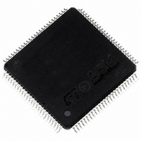
ST92F250CV2TB STMicroelectronics, ST92F250CV2TB Datasheet - Page 195

ST92F250CV2TB
Manufacturer Part Number
ST92F250CV2TB
Description
IC MCU 256K FLASH 100-TQFP
Manufacturer
STMicroelectronics
Series
ST9r
Datasheet
1.ST92F150CV1TB.pdf
(429 pages)
Specifications of ST92F250CV2TB
Core Processor
ST9
Core Size
8/16-Bit
Speed
24MHz
Connectivity
CAN, I²C, LIN, SCI, SPI
Peripherals
DMA, LVD, POR, PWM, WDT
Number Of I /o
80
Program Memory Size
256KB (256K x 8)
Program Memory Type
FLASH
Eeprom Size
1K x 8
Ram Size
8K x 8
Voltage - Supply (vcc/vdd)
4.5 V ~ 5.5 V
Data Converters
A/D 16x10b
Oscillator Type
Internal
Operating Temperature
-40°C ~ 105°C
Package / Case
100-TQFP, 100-VQFP
Processor Series
ST92F25x
Core
ST9
Data Bus Width
8 bit, 16 bit
Data Ram Size
8 KB
Interface Type
CAN, I2C, SCI, SPI
Maximum Clock Frequency
24 MHz
Number Of Programmable I/os
80
Number Of Timers
5 x 16 bit
Operating Supply Voltage
4.5 V to 5.5 V
Maximum Operating Temperature
+ 105 C
Mounting Style
SMD/SMT
Development Tools By Supplier
ST92F150-EPB
Minimum Operating Temperature
- 40 C
On-chip Adc
16 bit x 10 bit
Lead Free Status / RoHS Status
Lead free / RoHS Compliant
Other names
497-2140
Available stocks
Company
Part Number
Manufacturer
Quantity
Price
- Current page: 195 of 429
- Download datasheet (8Mb)
MULTIFUNCTION TIMER (Cont’d)
10.4.3.9 TxINA = Clock Up - TxINB = Clock
Down
The edge received on input pin A (or B) performs a
one step up (or down) count, so that the counter
clock and the up/down control are external. Setting
the UDC bit in the TCR register has no effect in
this configuration, and input pin B has priority on
input pin A.
10.4.3.10 TxINA = Up/Down - TxINB = Ext Clock
An High (or Low) level applied to input pin A sets
the counter in the up (or down) count mode, while
the signal applied to input pin B is used as clock for
the prescaler. Setting the UDC bit in the TCR reg-
ister has no effect in this configuration.
10.4.3.11 TxINA = Trigger Up - TxINB = Trigger
Down
Up/down control is performed through both input
pins A and B. A edge on input pin A sets the up
count mode, while a edge on input pin B (which
has priority on input pin A) sets the down count
mode. The counter clock is internally generated,
and setting the UDC bit in the TCR register has no
effect in this configuration.
10.4.3.12 TxINA = Up/Down - TxINB = I/O
An High (or Low) level of the signal applied on in-
put pin A sets the counter in the up (or down) count
mode. The counter clock is internally generated.
Setting the UDC bit in the TCR register has no ef-
fect in this configuration.
MULTIFUNCTION TIMER (MFT)
195/429
9
Related parts for ST92F250CV2TB
Image
Part Number
Description
Manufacturer
Datasheet
Request
R

Part Number:
Description:
STMicroelectronics [RIPPLE-CARRY BINARY COUNTER/DIVIDERS]
Manufacturer:
STMicroelectronics
Datasheet:

Part Number:
Description:
STMicroelectronics [LIQUID-CRYSTAL DISPLAY DRIVERS]
Manufacturer:
STMicroelectronics
Datasheet:

Part Number:
Description:
BOARD EVAL FOR MEMS SENSORS
Manufacturer:
STMicroelectronics
Datasheet:

Part Number:
Description:
NPN TRANSISTOR POWER MODULE
Manufacturer:
STMicroelectronics
Datasheet:

Part Number:
Description:
TURBOSWITCH ULTRA-FAST HIGH VOLTAGE DIODE
Manufacturer:
STMicroelectronics
Datasheet:

Part Number:
Description:
Manufacturer:
STMicroelectronics
Datasheet:

Part Number:
Description:
DIODE / SCR MODULE
Manufacturer:
STMicroelectronics
Datasheet:

Part Number:
Description:
DIODE / SCR MODULE
Manufacturer:
STMicroelectronics
Datasheet:

Part Number:
Description:
Search -----> STE16N100
Manufacturer:
STMicroelectronics
Datasheet:

Part Number:
Description:
Search ---> STE53NA50
Manufacturer:
STMicroelectronics
Datasheet:

Part Number:
Description:
NPN Transistor Power Module
Manufacturer:
STMicroelectronics
Datasheet:

Part Number:
Description:
DIODE / SCR MODULE
Manufacturer:
STMicroelectronics
Datasheet:


