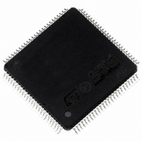
ST92F250CV2TB STMicroelectronics, ST92F250CV2TB Datasheet - Page 418

ST92F250CV2TB
Manufacturer Part Number
ST92F250CV2TB
Description
IC MCU 256K FLASH 100-TQFP
Manufacturer
STMicroelectronics
Series
ST9r
Datasheet
1.ST92F150CV1TB.pdf
(429 pages)
Specifications of ST92F250CV2TB
Core Processor
ST9
Core Size
8/16-Bit
Speed
24MHz
Connectivity
CAN, I²C, LIN, SCI, SPI
Peripherals
DMA, LVD, POR, PWM, WDT
Number Of I /o
80
Program Memory Size
256KB (256K x 8)
Program Memory Type
FLASH
Eeprom Size
1K x 8
Ram Size
8K x 8
Voltage - Supply (vcc/vdd)
4.5 V ~ 5.5 V
Data Converters
A/D 16x10b
Oscillator Type
Internal
Operating Temperature
-40°C ~ 105°C
Package / Case
100-TQFP, 100-VQFP
Processor Series
ST92F25x
Core
ST9
Data Bus Width
8 bit, 16 bit
Data Ram Size
8 KB
Interface Type
CAN, I2C, SCI, SPI
Maximum Clock Frequency
24 MHz
Number Of Programmable I/os
80
Number Of Timers
5 x 16 bit
Operating Supply Voltage
4.5 V to 5.5 V
Maximum Operating Temperature
+ 105 C
Mounting Style
SMD/SMT
Development Tools By Supplier
ST92F150-EPB
Minimum Operating Temperature
- 40 C
On-chip Adc
16 bit x 10 bit
Lead Free Status / RoHS Status
Lead free / RoHS Compliant
Other names
497-2140
Available stocks
Company
Part Number
Manufacturer
Quantity
Price
- Current page: 418 of 429
- Download datasheet (8Mb)
ST92F124/F150/F250 - KNOWN LIMITATIONS
KNOWN LIMITATIONS (Cont’d)
Workaround 2
Workaround 2 (see
FMP=2 and the CAN cell is receiving, if not the
FIFO can be released immediately. If yes, the pro-
gram goes through a sequence of test instructions
on the RX pin that last longer than the time be-
tween the acknowledge dominant bit and the crit-
ical time slot. If the Rx pin is in recessive state for
more than 8 CAN bit times, it means we are now
Figure 6. Reception with TCAN=12/f
Figure 7. Workaround 2 in Assembler
418/429
1
asm (“
_release:
“);
Sampling of Rx pin
CAN Bus signal
spp #48
ld
and
cp
jxnz
pushw RR232
srp
btjf
btjf
btjf
btjf
btjf
btjf
btjf
btjf
btjf
btjf
btjf
btjf
popw
r0, R244
r0, #3
r0, #2
_release
#31
r1.5, _release
r12.3, _release
r12.3, _release
r12.3, _release
r12.3, _release
r12.3, _release
r12.3, _release
r12.3, _release
r12.3, _release
r12.3, _release
r12.3, _release
r12.3, _release
or R244, #32
RR232
Figure
R R R
7) first tests that
/*
/* set CAN0_CTRL page
/* Use spp #36 for CAN1
/* For FIFO 0
/* NB: Replace R244 with R245 for FIFO 1
/*
/*
/* (JRNE instruction)
/* if FMP is not 2 then FIFO
/* release can be done
/* push working group
/* set group F as working group
/* REC bit of CMSR register
/* sample RX bit for 8 bit time
/* ie. 11 btjf instructions
/*
/*
/*
/*
/*
/*
/*
/*
/*
/*
/* NB: Replace R244 with R245 for FIFO 1
/* restore previous working group
D
CPU
R R R
set RFOM bit of CRFR0 register
and sampling time is 16/f
D
after the acknowledge and the critical slot. If a
dominant bit is read on the bus, we can release the
FIFO immediately. This workaround has to be
written in assembly language to avoid the compiler
optimizing the test sequence.
The implementation shown here is for the CAN
bus maximum speed (1MBd @ 8MHz CPU clock).
R R R
D
CPU
Bytes/cycles
R R R
2/4
2/4
3/6
3/6
2/6
2/8 or 10
2/4
3/6 or 10 if jmp
3/6 or 10 if jmp
3/6 or 10 if jmp
3/6 or 10 if jmp
3/6 or 10 if jmp
3/6 or 10 if jmp
3/6 or 10 if jmp
3/6 or 10 if jmp
3/6 or 10 if jmp
3/6 or 10 if jmp
3/6 or 10 if jmp
3/6 or 10 if jmp
3/6
2/10
D
R R R
D
*/
*/
*/
*/
*/
*/
*/
*/
*/
*/
*/
*/
*/
*/
*/
*/
*/
*/
*/
*/
*/
*/
*/
*/
*/
*/
Related parts for ST92F250CV2TB
Image
Part Number
Description
Manufacturer
Datasheet
Request
R

Part Number:
Description:
STMicroelectronics [RIPPLE-CARRY BINARY COUNTER/DIVIDERS]
Manufacturer:
STMicroelectronics
Datasheet:

Part Number:
Description:
STMicroelectronics [LIQUID-CRYSTAL DISPLAY DRIVERS]
Manufacturer:
STMicroelectronics
Datasheet:

Part Number:
Description:
BOARD EVAL FOR MEMS SENSORS
Manufacturer:
STMicroelectronics
Datasheet:

Part Number:
Description:
NPN TRANSISTOR POWER MODULE
Manufacturer:
STMicroelectronics
Datasheet:

Part Number:
Description:
TURBOSWITCH ULTRA-FAST HIGH VOLTAGE DIODE
Manufacturer:
STMicroelectronics
Datasheet:

Part Number:
Description:
Manufacturer:
STMicroelectronics
Datasheet:

Part Number:
Description:
DIODE / SCR MODULE
Manufacturer:
STMicroelectronics
Datasheet:

Part Number:
Description:
DIODE / SCR MODULE
Manufacturer:
STMicroelectronics
Datasheet:

Part Number:
Description:
Search -----> STE16N100
Manufacturer:
STMicroelectronics
Datasheet:

Part Number:
Description:
Search ---> STE53NA50
Manufacturer:
STMicroelectronics
Datasheet:

Part Number:
Description:
NPN Transistor Power Module
Manufacturer:
STMicroelectronics
Datasheet:

Part Number:
Description:
DIODE / SCR MODULE
Manufacturer:
STMicroelectronics
Datasheet:


