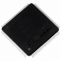
ST92F250CV2TB STMicroelectronics, ST92F250CV2TB Datasheet - Page 284

ST92F250CV2TB
Manufacturer Part Number
ST92F250CV2TB
Description
IC MCU 256K FLASH 100-TQFP
Manufacturer
STMicroelectronics
Series
ST9r
Datasheet
1.ST92F150CV1TB.pdf
(429 pages)
Specifications of ST92F250CV2TB
Core Processor
ST9
Core Size
8/16-Bit
Speed
24MHz
Connectivity
CAN, I²C, LIN, SCI, SPI
Peripherals
DMA, LVD, POR, PWM, WDT
Number Of I /o
80
Program Memory Size
256KB (256K x 8)
Program Memory Type
FLASH
Eeprom Size
1K x 8
Ram Size
8K x 8
Voltage - Supply (vcc/vdd)
4.5 V ~ 5.5 V
Data Converters
A/D 16x10b
Oscillator Type
Internal
Operating Temperature
-40°C ~ 105°C
Package / Case
100-TQFP, 100-VQFP
Processor Series
ST92F25x
Core
ST9
Data Bus Width
8 bit, 16 bit
Data Ram Size
8 KB
Interface Type
CAN, I2C, SCI, SPI
Maximum Clock Frequency
24 MHz
Number Of Programmable I/os
80
Number Of Timers
5 x 16 bit
Operating Supply Voltage
4.5 V to 5.5 V
Maximum Operating Temperature
+ 105 C
Mounting Style
SMD/SMT
Development Tools By Supplier
ST92F150-EPB
Minimum Operating Temperature
- 40 C
On-chip Adc
16 bit x 10 bit
Lead Free Status / RoHS Status
Lead free / RoHS Compliant
Other names
497-2140
Available stocks
Company
Part Number
Manufacturer
Quantity
Price
- Current page: 284 of 429
- Download datasheet (8Mb)
J1850 Byte Level Protocol Decoder (JBLPD)
10.9 J1850 Byte Level Protocol Decoder (JBLPD)
10.9.1 Introduction
The JBLPD is used to exchange data between the
ST9 microcontroller and an external J1850 trans-
ceiver I.C.
The JBLPD transmits a string of variable pulse
width (VPW) symbols to the transceiver. It also re-
ceives VPW encoded symbols from the transceiv-
er, decodes them and places the data in a register.
In-frame responses of type 0, 1, 2 and 3 are sup-
ported and the appropriate normalization bit is
generated automatically. The JBLPD filters out
any incoming messages which it does not care to
receive. It also includes a programmable external
loop delay.
The JBLPD uses two signals to communicate with
the transceiver:
– VPWI (input)
– VPWO (output)
284/429
9
10.9.2 Main Features
■
■
■
■
■
■
■
■
■
■
■
■
■
■
SAE J1850 compatible
Digital filter
In-Frame Responses of type 0, 1, 2, 3 supported
with automatic normalization bit
Programmable External Loop Delay
Diagnostic 4x time mode
Diagnostic Local Loopback mode
Wide range of MCU internal frequencies
allowed
Low
suspended)
Very low power consumption mode (JBLPD
disabled)
Don’t care message filter
Selectable VPWI input polarity
Selectable Normalization Bit symbol form
6 maskable interrupts
DMA transmission and reception with End Of
Block interrupts
power
consumption
mode
(JBLPD
Related parts for ST92F250CV2TB
Image
Part Number
Description
Manufacturer
Datasheet
Request
R

Part Number:
Description:
STMicroelectronics [RIPPLE-CARRY BINARY COUNTER/DIVIDERS]
Manufacturer:
STMicroelectronics
Datasheet:

Part Number:
Description:
STMicroelectronics [LIQUID-CRYSTAL DISPLAY DRIVERS]
Manufacturer:
STMicroelectronics
Datasheet:

Part Number:
Description:
BOARD EVAL FOR MEMS SENSORS
Manufacturer:
STMicroelectronics
Datasheet:

Part Number:
Description:
NPN TRANSISTOR POWER MODULE
Manufacturer:
STMicroelectronics
Datasheet:

Part Number:
Description:
TURBOSWITCH ULTRA-FAST HIGH VOLTAGE DIODE
Manufacturer:
STMicroelectronics
Datasheet:

Part Number:
Description:
Manufacturer:
STMicroelectronics
Datasheet:

Part Number:
Description:
DIODE / SCR MODULE
Manufacturer:
STMicroelectronics
Datasheet:

Part Number:
Description:
DIODE / SCR MODULE
Manufacturer:
STMicroelectronics
Datasheet:

Part Number:
Description:
Search -----> STE16N100
Manufacturer:
STMicroelectronics
Datasheet:

Part Number:
Description:
Search ---> STE53NA50
Manufacturer:
STMicroelectronics
Datasheet:

Part Number:
Description:
NPN Transistor Power Module
Manufacturer:
STMicroelectronics
Datasheet:

Part Number:
Description:
DIODE / SCR MODULE
Manufacturer:
STMicroelectronics
Datasheet:


