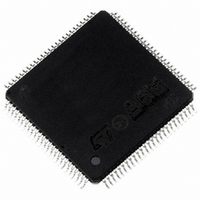
ST92F250CV2TB STMicroelectronics, ST92F250CV2TB Datasheet - Page 356

ST92F250CV2TB
Manufacturer Part Number
ST92F250CV2TB
Description
IC MCU 256K FLASH 100-TQFP
Manufacturer
STMicroelectronics
Series
ST9r
Datasheet
1.ST92F150CV1TB.pdf
(429 pages)
Specifications of ST92F250CV2TB
Core Processor
ST9
Core Size
8/16-Bit
Speed
24MHz
Connectivity
CAN, I²C, LIN, SCI, SPI
Peripherals
DMA, LVD, POR, PWM, WDT
Number Of I /o
80
Program Memory Size
256KB (256K x 8)
Program Memory Type
FLASH
Eeprom Size
1K x 8
Ram Size
8K x 8
Voltage - Supply (vcc/vdd)
4.5 V ~ 5.5 V
Data Converters
A/D 16x10b
Oscillator Type
Internal
Operating Temperature
-40°C ~ 105°C
Package / Case
100-TQFP, 100-VQFP
Processor Series
ST92F25x
Core
ST9
Data Bus Width
8 bit, 16 bit
Data Ram Size
8 KB
Interface Type
CAN, I2C, SCI, SPI
Maximum Clock Frequency
24 MHz
Number Of Programmable I/os
80
Number Of Timers
5 x 16 bit
Operating Supply Voltage
4.5 V to 5.5 V
Maximum Operating Temperature
+ 105 C
Mounting Style
SMD/SMT
Development Tools By Supplier
ST92F150-EPB
Minimum Operating Temperature
- 40 C
On-chip Adc
16 bit x 10 bit
Lead Free Status / RoHS Status
Lead free / RoHS Compliant
Other names
497-2140
Available stocks
Company
Part Number
Manufacturer
Quantity
Price
- Current page: 356 of 429
- Download datasheet (8Mb)
CONTROLLER AREA NETWORK (bxCAN)
CONTROLLER AREA NETWORK (Cont’d)
Bit 2 = FML1 Filter Mode Low
Mode of the low registers of filter 1.
0: Low registers are in mask mode
1: Low registers are in identifier list mode
Bit 1 = FMH0 Filter Mode High
Mode of the high registers of filter 0.
0: High registers are in mask mode
1: High registers are in identifier list mode
Bit 0 = FML0 Filter Mode Low
Mode of the low registers of filter 0.
0: Low registers are in mask mode
1: Low registers are in identifier list mode
356/429
9
FILTER x REGISTER[7:0] (CFxR[7:0])
Read / Write
Reset Value: xxxx xxxx (xxh)
In all configurations:
Bit 7:0 = FB[7:0] Filter Bits
Identifier
Each bit of the register specifies the level of the
corresponding bit of the expected identifier.
0: Dominant bit is expected
1: Recessive bit is expected
Mask
Each bit of the register specifies whether the bit of
the associated identifier register must match with
the corresponding bit of the expected identifier or
not.
0: Don’t care, the bit is not used for the comparison
1: Must match, the bit of the incoming identifier
Note: Each filter x is composed of 8 registers,
CFxR[7:0]. Depending on the scale and mode
configuration of the filter the function of each reg-
ister can differ. For the filter mapping, functions
description and mask registers association, refer
to Section
A Mask/Identifier register in mask mode has the
same bit mapping as in identifier list mode.
Note: To modify these registers, the correspond-
ing FACT bit in the CFCR register must be
cleared.
FB7
must have the same level has specified in the
corresponding identifier register of the filter.
7
FB6
10.10.5.4Identifier
FB5
FB4
FB3
Filtering.
FB2
FB1
FB0
0
Related parts for ST92F250CV2TB
Image
Part Number
Description
Manufacturer
Datasheet
Request
R

Part Number:
Description:
STMicroelectronics [RIPPLE-CARRY BINARY COUNTER/DIVIDERS]
Manufacturer:
STMicroelectronics
Datasheet:

Part Number:
Description:
STMicroelectronics [LIQUID-CRYSTAL DISPLAY DRIVERS]
Manufacturer:
STMicroelectronics
Datasheet:

Part Number:
Description:
BOARD EVAL FOR MEMS SENSORS
Manufacturer:
STMicroelectronics
Datasheet:

Part Number:
Description:
NPN TRANSISTOR POWER MODULE
Manufacturer:
STMicroelectronics
Datasheet:

Part Number:
Description:
TURBOSWITCH ULTRA-FAST HIGH VOLTAGE DIODE
Manufacturer:
STMicroelectronics
Datasheet:

Part Number:
Description:
Manufacturer:
STMicroelectronics
Datasheet:

Part Number:
Description:
DIODE / SCR MODULE
Manufacturer:
STMicroelectronics
Datasheet:

Part Number:
Description:
DIODE / SCR MODULE
Manufacturer:
STMicroelectronics
Datasheet:

Part Number:
Description:
Search -----> STE16N100
Manufacturer:
STMicroelectronics
Datasheet:

Part Number:
Description:
Search ---> STE53NA50
Manufacturer:
STMicroelectronics
Datasheet:

Part Number:
Description:
NPN Transistor Power Module
Manufacturer:
STMicroelectronics
Datasheet:

Part Number:
Description:
DIODE / SCR MODULE
Manufacturer:
STMicroelectronics
Datasheet:


