Z8F3201VN020EC00TR Zilog, Z8F3201VN020EC00TR Datasheet - Page 141
Z8F3201VN020EC00TR
Manufacturer Part Number
Z8F3201VN020EC00TR
Description
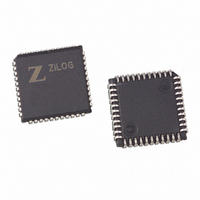
IC ENCORE MCU FLASH 32K 44PLCC
Manufacturer
Zilog
Series
Encore!®r
Datasheet
1.Z8F1601VN020EC.pdf
(246 pages)
Specifications of Z8F3201VN020EC00TR
Core Processor
Z8
Core Size
8-Bit
Speed
20MHz
Connectivity
I²C, IrDA, SPI, UART/USART
Peripherals
Brown-out Detect/Reset, DMA, POR, PWM, WDT
Number Of I /o
31
Program Memory Size
32KB (32K x 8)
Program Memory Type
FLASH
Ram Size
2K x 8
Voltage - Supply (vcc/vdd)
3 V ~ 3.6 V
Data Converters
A/D 8x10b
Oscillator Type
Internal
Operating Temperature
-40°C ~ 105°C
Package / Case
44-LCC (J-Lead)
Lead Free Status / RoHS Status
Contains lead / RoHS non-compliant
Eeprom Size
-
Other names
Z8F3201VN020EC00T
Available stocks
Company
Part Number
Manufacturer
Quantity
Price


PS017610-0404
Configuring DMA0 and DMA1 for Data Transfer
DMA_ADC Operation
Follow these steps to configure and enable DMA0 or DMA1:
1. Write to the DMAx I/O Address register to set the Register File address identifying the
2. Determine the 12-bit Start and End Register File addresses. The 12-bit Start Address
3. Write the Start and End Register File address high nibbles to the DMAx End/Start
4. Write the lower byte of the Start Address to the DMAx Start/Current Address register.
5. Write the lower byte of the End Address to the DMAx End Address register.
6. Write to the DMAx Control register to complete the following:
DMA_ADC transfers data from the ADC to the Register File. The sequence of operations
in a DMA_ADC data transfer is:
1. ADC completes conversion on the current ADC input channel and signals the DMA
2. DMA_ADC requests control of the system bus (address and data) from the eZ8 CPU.
3. After the eZ8 CPU acknowledges the bus request, DMA_ADC transfers the two-byte
4. If the current ADC Analog Input is the highest numbered input to be converted:
on-chip peripheral control register. The upper nibble of the 12-bit address for on-chip
peripheral control registers is always
is given by {DMAx_H[3:0], DMA_START[7:0]}. The 12-bit End Address is given by
{DMAx_H[7:4], DMA_END[7:0]}.
Address High Nibble register.
–
–
–
–
–
–
controller that two-bytes of ADC data are ready for transfer.
ADC output value to the Register File and then returns system bus control back to the
eZ8 CPU.
–
–
Select loop or single-pass mode operation
Select the data transfer direction (either from the Register File RAM to the on-
chip peripheral control register; or from the on-chip peripheral control register to
the Register File RAM)
Enable the DMAx interrupt request, if desired
Select Word or Byte mode
Select the DMAx request trigger
Enable the DMAx channel
DMA_ADC resets the ADC Analog Input number to 0 and initiates data
conversion on ADC Analog Input 0.
If configured to generate an interrupt, DMA_ADC sends an interrupt request to
the Interrupt Controller
Z8F640x/Z8F480x/Z8F320x/Z8F240x/Z8F160x
FH
. The full address is {FH, DMAx_IO[7:0]}
Direct Memory Access Controller
Z8 Encore!
®
123
Related parts for Z8F3201VN020EC00TR
Image
Part Number
Description
Manufacturer
Datasheet
Request
R

Part Number:
Description:
Communication Controllers, ZILOG INTELLIGENT PERIPHERAL CONTROLLER (ZIP)
Manufacturer:
Zilog, Inc.
Datasheet:

Part Number:
Description:
KIT DEV FOR Z8 ENCORE 16K TO 64K
Manufacturer:
Zilog
Datasheet:

Part Number:
Description:
KIT DEV Z8 ENCORE XP 28-PIN
Manufacturer:
Zilog
Datasheet:

Part Number:
Description:
DEV KIT FOR Z8 ENCORE 8K/4K
Manufacturer:
Zilog
Datasheet:

Part Number:
Description:
KIT DEV Z8 ENCORE XP 28-PIN
Manufacturer:
Zilog
Datasheet:

Part Number:
Description:
DEV KIT FOR Z8 ENCORE 4K TO 8K
Manufacturer:
Zilog
Datasheet:
Part Number:
Description:
CMOS Z8 microcontroller. ROM 16 Kbytes, RAM 256 bytes, speed 16 MHz, 32 lines I/O, 3.0V to 5.5V
Manufacturer:
Zilog, Inc.
Datasheet:
Part Number:
Description:
Low-cost microcontroller. 512 bytes ROM, 61 bytes RAM, 8 MHz
Manufacturer:
Zilog, Inc.
Datasheet:
Part Number:
Description:
Z8 4K OTP Microcontroller
Manufacturer:
Zilog, Inc.
Datasheet:
Part Number:
Description:
CMOS SUPER8 ROMLESS MCU
Manufacturer:
Zilog, Inc.
Datasheet:
Part Number:
Description:
SL1866 CMOSZ8 OTP Microcontroller
Manufacturer:
Zilog, Inc.
Datasheet:
Part Number:
Description:
SL1866 CMOSZ8 OTP Microcontroller
Manufacturer:
Zilog, Inc.
Datasheet:
Part Number:
Description:
OTP (KB) = 1, RAM = 125, Speed = 12, I/O = 14, 8-bit Timers = 2, Comm Interfaces Other Features = Por, LV Protect, Voltage = 4.5-5.5V
Manufacturer:
Zilog, Inc.
Datasheet:
Part Number:
Description:
Manufacturer:
Zilog, Inc.
Datasheet: