R8A77850ADBGV Renesas Electronics America, R8A77850ADBGV Datasheet - Page 1238
R8A77850ADBGV
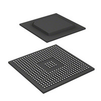
Manufacturer Part Number
R8A77850ADBGV
Description
IC SUPERH MPU ROMLESS 436-BGA
Manufacturer
Renesas Electronics America
Series
SuperH® SH7780r
Datasheet
1.R8A77850AADBGV.pdf
(1694 pages)
Specifications of R8A77850ADBGV
Core Processor
SH-4A
Core Size
32-Bit
Speed
600MHz
Connectivity
Audio Codec, MMC, Serial Sound, SCI, SIO, SPI, SSI
Peripherals
DMA, POR, WDT
Number Of I /o
108
Program Memory Type
ROMless
Ram Size
8K x 8
Voltage - Supply (vcc/vdd)
1 V ~ 1.2 V
Oscillator Type
External
Operating Temperature
-40°C ~ 85°C
Package / Case
436-BGA
Lead Free Status / RoHS Status
Lead free / RoHS Compliant
Eeprom Size
-
Program Memory Size
-
Data Converters
-
Available stocks
Company
Part Number
Manufacturer
Quantity
Price
Company:

Part Number:
R8A77850ADBGV
Manufacturer:
Renesas Electronics America
Quantity:
10 000
Company:
Part Number:
R8A77850ADBGV#RD0Z
Manufacturer:
Renesas Electronics America
Quantity:
10 000


24. Multimedia Card Interface (MMCIF)
24.3.16 Data Register (DR)
DR is a register for reading/writing FIFO data.
Word/byte access is enabled to addresses of this register.
The following shows examples of DR access.
When data is written to DR in the following steps 1 to 4, the transmit data is stored in the FIFO as
shown in figure 24.2.
1. Write word data H'0123 to DR.
2. Write byte data H'45 to DR.
3. Write word data H'6789 to DR.
4. Write byte data H'AB to DR.
When the receive data is stored in the FIFO as shown in figure 24.2 (for example, after data is
started to be received while the FIFO is empty and data is received in the order of H'01, H'23, ...,
H'AB), data can be read from DR in the following steps 5 to 8.
5. Read byte data H'01 from DR.
6. Read word data H'2345 from DR.
7. Read byte data H'67 from DR.
8. Read word data H'89AB from DR.
Rev.1.00 Jan. 10, 2008 Page 1206 of 1658
REJ09B0261-0100
Initial value:
Bit
15 to 0
R/W:
Bit:
Bit Name
DR
R/W
15
—
R/W
14
—
R/W
13
—
Initial
Value
⎯
R/W
12
—
R/W
11
—
R/W
R/W
R/W
10
—
Description
Register for reading/writing FIFO data.
Word/byte access is enabled.
When DR is accessed in words, the upper and lower
bytes are transmitted or received in that order. Word
access and byte access can be done in random order.
However, (DR address + 1) cannot be accessed in
bytes.
R/W
—
9
R/W
—
8
DR
R/W
—
7
R/W
—
6
R/W
—
5
R/W
—
4
R/W R/W
3
—
—
2
R/W
—
1
R/W
—
0
Related parts for R8A77850ADBGV
Image
Part Number
Description
Manufacturer
Datasheet
Request
R

Part Number:
Description:
KIT STARTER FOR M16C/29
Manufacturer:
Renesas Electronics America
Datasheet:

Part Number:
Description:
KIT STARTER FOR R8C/2D
Manufacturer:
Renesas Electronics America
Datasheet:

Part Number:
Description:
R0K33062P STARTER KIT
Manufacturer:
Renesas Electronics America
Datasheet:

Part Number:
Description:
KIT STARTER FOR R8C/23 E8A
Manufacturer:
Renesas Electronics America
Datasheet:

Part Number:
Description:
KIT STARTER FOR R8C/25
Manufacturer:
Renesas Electronics America
Datasheet:

Part Number:
Description:
KIT STARTER H8S2456 SHARPE DSPLY
Manufacturer:
Renesas Electronics America
Datasheet:

Part Number:
Description:
KIT STARTER FOR R8C38C
Manufacturer:
Renesas Electronics America
Datasheet:

Part Number:
Description:
KIT STARTER FOR R8C35C
Manufacturer:
Renesas Electronics America
Datasheet:

Part Number:
Description:
KIT STARTER FOR R8CL3AC+LCD APPS
Manufacturer:
Renesas Electronics America
Datasheet:
Part Number:
Description:
KIT STARTER FOR RX610
Manufacturer:
Renesas Electronics America
Datasheet:

Part Number:
Description:
KIT STARTER FOR R32C/118
Manufacturer:
Renesas Electronics America
Datasheet:

Part Number:
Description:
KIT DEV RSK-R8C/26-29
Manufacturer:
Renesas Electronics America
Datasheet:

Part Number:
Description:
KIT STARTER FOR SH7124
Manufacturer:
Renesas Electronics America
Datasheet:

Part Number:
Description:
KIT STARTER FOR H8SX/1622
Manufacturer:
Renesas Electronics America
Datasheet:

Part Number:
Description:
KIT DEV FOR SH7203
Manufacturer:
Renesas Electronics America
Datasheet: