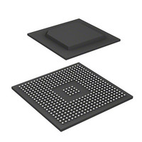
R8A77850ADBGV Renesas Electronics America, R8A77850ADBGV Datasheet - Page 1367

R8A77850ADBGV
Manufacturer Part Number
R8A77850ADBGV
Description
IC SUPERH MPU ROMLESS 436-BGA
Manufacturer
Renesas Electronics America
Series
SuperH® SH7780r
Datasheet
1.R8A77850AADBGV.pdf
(1694 pages)
Specifications of R8A77850ADBGV
Core Processor
SH-4A
Core Size
32-Bit
Speed
600MHz
Connectivity
Audio Codec, MMC, Serial Sound, SCI, SIO, SPI, SSI
Peripherals
DMA, POR, WDT
Number Of I /o
108
Program Memory Type
ROMless
Ram Size
8K x 8
Voltage - Supply (vcc/vdd)
1 V ~ 1.2 V
Oscillator Type
External
Operating Temperature
-40°C ~ 85°C
Package / Case
436-BGA
Lead Free Status / RoHS Status
Lead free / RoHS Compliant
Eeprom Size
-
Program Memory Size
-
Data Converters
-
Available stocks
Company
Part Number
Manufacturer
Quantity
Price
Company:
Part Number:
R8A77850ADBGV
Manufacturer:
Renesas Electronics America
Quantity:
10 000
Company:
Part Number:
R8A77850ADBGV#RD0Z
Manufacturer:
Renesas Electronics America
Quantity:
10 000
- Current page: 1367 of 1694
- Download datasheet (9Mb)
26.5
26.5.1
If an overflow occurs during receive DMA operation, the module must be reactivated.
The receive buffer of SSI has 32-bit common register to the left channel and right channel. If an
overflow occurs under the condition of control register (SSICR) data-word length (DWL2 to 0) is
32-bit and system-word length (SWL2 to 0) is 32-bit, SSI has received the data at right channel
that should be received at left channel.
If an overflow occurrence is confirmed through an overflow error interrupt or overflow error status
flag (the OIRQ bit in SSISR), disable the DMA transfer of the SSI to halt its operation by writing
0 to the EN bit and DMEN bit in SSICR (then terminate the DMAC setting). And clear the
overflow status flag by writing 0 to the OIRQ bit, set the DMA again to restart transfer.
26.5.2
Before setting or activating the SSI module, set the peripheral module select registers and the port
control registers in terms of the SSI0 and SSI1 channels as described in section 28, General
Purpose I/O Ports (GPIO).
26.5.3
When terminating data transmission in slave mode, the WS signal (SSI WS) input should be kept
the active state until SSICR.IDST becomes 1 after SSICR.EN is cleared to 0 (see next page
figure). The “active state” means the WS signal is being input high (or low) and low (or high)
alternately as for each system word cycles (it will become more than five system word cycles after
EN bit is cleared to 0).
If the WS signal active state input is stopped before SSICR.IDST becomes 1, the transfer of the
SSI is not terminated normally and the transfer will be suspended. If SSICR.EN is set to 1 again in
this state, the transfer is resumed from the suspended state and an unexpected data transfer may
occur.
Note that, the normal data transmission of the SSI can be resumed from the first or second WS
falling edge after the EN bit is set to 1 while the IDST bit is 1.
Usage Note
Restrictions when an Overflow Occurs during Receive DMA Operation
Pin Function Setting for the SSI Module
Usage Note in Slave Mode
Rev.1.00 Jan. 10, 2008 Page 1335 of 1658
26. Serial Sound Interface (SSI) Module
REJ09B0261-0100
Related parts for R8A77850ADBGV
Image
Part Number
Description
Manufacturer
Datasheet
Request
R

Part Number:
Description:
KIT STARTER FOR M16C/29
Manufacturer:
Renesas Electronics America
Datasheet:

Part Number:
Description:
KIT STARTER FOR R8C/2D
Manufacturer:
Renesas Electronics America
Datasheet:

Part Number:
Description:
R0K33062P STARTER KIT
Manufacturer:
Renesas Electronics America
Datasheet:

Part Number:
Description:
KIT STARTER FOR R8C/23 E8A
Manufacturer:
Renesas Electronics America
Datasheet:

Part Number:
Description:
KIT STARTER FOR R8C/25
Manufacturer:
Renesas Electronics America
Datasheet:

Part Number:
Description:
KIT STARTER H8S2456 SHARPE DSPLY
Manufacturer:
Renesas Electronics America
Datasheet:

Part Number:
Description:
KIT STARTER FOR R8C38C
Manufacturer:
Renesas Electronics America
Datasheet:

Part Number:
Description:
KIT STARTER FOR R8C35C
Manufacturer:
Renesas Electronics America
Datasheet:

Part Number:
Description:
KIT STARTER FOR R8CL3AC+LCD APPS
Manufacturer:
Renesas Electronics America
Datasheet:

Part Number:
Description:
KIT STARTER FOR RX610
Manufacturer:
Renesas Electronics America
Datasheet:

Part Number:
Description:
KIT STARTER FOR R32C/118
Manufacturer:
Renesas Electronics America
Datasheet:

Part Number:
Description:
KIT DEV RSK-R8C/26-29
Manufacturer:
Renesas Electronics America
Datasheet:

Part Number:
Description:
KIT STARTER FOR SH7124
Manufacturer:
Renesas Electronics America
Datasheet:

Part Number:
Description:
KIT STARTER FOR H8SX/1622
Manufacturer:
Renesas Electronics America
Datasheet:

Part Number:
Description:
KIT DEV FOR SH7203
Manufacturer:
Renesas Electronics America
Datasheet:


