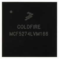
MCF5274LVM166 Freescale Semiconductor, MCF5274LVM166 Datasheet - Page 26

MCF5274LVM166
Manufacturer Part Number
MCF5274LVM166
Description
IC MPU 32BIT COLDF 196-MAPBGA
Manufacturer
Freescale Semiconductor
Series
MCF527xr
Datasheet
1.MCF5274LVM166J.pdf
(44 pages)
Specifications of MCF5274LVM166
Core Processor
Coldfire V2
Core Size
32-Bit
Speed
166MHz
Connectivity
EBI/EMI, Ethernet, I²C, SPI, UART/USART, USB
Peripherals
DMA, WDT
Number Of I /o
61
Program Memory Type
ROMless
Ram Size
64K x 8
Voltage - Supply (vcc/vdd)
1.4 V ~ 1.6 V
Oscillator Type
External
Operating Temperature
0°C ~ 70°C
Package / Case
196-MAPBGA
Embedded Interface Type
I2C, SPI, USB, UART
Digital Ic Case Style
BGA
No. Of Pins
196
Operating Temperature Range
0°C To +70°C
Frequency Typ
166MHz
Rohs Compliant
Yes
Family Name
MCF5xxx
Device Core
ColdFire
Device Core Size
32b
Frequency (max)
166MHz
Instruction Set Architecture
RISC
Operating Supply Voltage (max)
1.6V
Operating Supply Voltage (min)
1.4V
Operating Temp Range
0C to 70C
Operating Temperature Classification
Commercial
Mounting
Surface Mount
Pin Count
196
Package Type
MA-BGA
Lead Free Status / RoHS Status
Lead free / RoHS Compliant
Eeprom Size
-
Program Memory Size
-
Data Converters
-
Lead Free Status / Rohs Status
Compliant
Available stocks
Company
Part Number
Manufacturer
Quantity
Price
Company:
Part Number:
MCF5274LVM166
Manufacturer:
FREESCALE
Quantity:
201
Company:
Part Number:
MCF5274LVM166
Manufacturer:
Freescale Semiconductor
Quantity:
10 000
Company:
Part Number:
MCF5274LVM166J
Manufacturer:
Freescale Semiconductor
Quantity:
10 000
Electrical Characteristics
Read/write bus timings listed in
26
1
B11
B12
B13
TSIZ[1:0]
A[23:0]
D[31:16]
Name
CS, BS, and OE transition after the falling edge of CLKOUT.
CLKOUT
BS[3:2]
TEA (H)
R/W
OE
TIP
CSn
TA
TS
(H)
(H)
CLKOUT high to data output (D[31:16]) valid
CLKOUT high to data output (D[31:16]) invalid
CLKOUT high to data output (D[31:16]) high impedance
B8
B8
B6a
B8
MCF5275 Integrated Microprocessor Family Hardware Specification, Rev. 4
Table 13. External Bus Output Timing Specifications (continued)
Figure 8. Read/Write (Internally Terminated) SRAM Bus Timing
B6b
B6c
S0
B9
Characteristic
S1
Table 13
B4
S2
B7a
B7
are shown in
S3
Data Outputs
B5
S4
B7
B8
B6b
B8
S5
Figure
B6a
t
t
t
S0
CHDOV
CHDOI
CHDOZ
Symbol
B8
B9
B11
8,
Figure
S1
9, and
S2
Min
B0
1.0
—
—
S3
Figure
B7a
S4
B7
Freescale Semiconductor
B9
B9
B12
B13
10.
B9
Max
—
9
9
S5
Unit
ns
ns
ns


