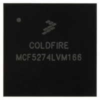
MCF5274LVM166 Freescale Semiconductor, MCF5274LVM166 Datasheet - Page 29

MCF5274LVM166
Manufacturer Part Number
MCF5274LVM166
Description
IC MPU 32BIT COLDF 196-MAPBGA
Manufacturer
Freescale Semiconductor
Series
MCF527xr
Datasheet
1.MCF5274LVM166J.pdf
(44 pages)
Specifications of MCF5274LVM166
Core Processor
Coldfire V2
Core Size
32-Bit
Speed
166MHz
Connectivity
EBI/EMI, Ethernet, I²C, SPI, UART/USART, USB
Peripherals
DMA, WDT
Number Of I /o
61
Program Memory Type
ROMless
Ram Size
64K x 8
Voltage - Supply (vcc/vdd)
1.4 V ~ 1.6 V
Oscillator Type
External
Operating Temperature
0°C ~ 70°C
Package / Case
196-MAPBGA
Embedded Interface Type
I2C, SPI, USB, UART
Digital Ic Case Style
BGA
No. Of Pins
196
Operating Temperature Range
0°C To +70°C
Frequency Typ
166MHz
Rohs Compliant
Yes
Family Name
MCF5xxx
Device Core
ColdFire
Device Core Size
32b
Frequency (max)
166MHz
Instruction Set Architecture
RISC
Operating Supply Voltage (max)
1.6V
Operating Supply Voltage (min)
1.4V
Operating Temp Range
0C to 70C
Operating Temperature Classification
Commercial
Mounting
Surface Mount
Pin Count
196
Package Type
MA-BGA
Lead Free Status / RoHS Status
Lead free / RoHS Compliant
Eeprom Size
-
Program Memory Size
-
Data Converters
-
Lead Free Status / Rohs Status
Compliant
Available stocks
Company
Part Number
Manufacturer
Quantity
Price
Company:
Part Number:
MCF5274LVM166
Manufacturer:
FREESCALE
Quantity:
201
Company:
Part Number:
MCF5274LVM166
Manufacturer:
Freescale Semiconductor
Quantity:
10 000
Company:
Part Number:
MCF5274LVM166J
Manufacturer:
Freescale Semiconductor
Quantity:
10 000
8.8
The DDR SDRAM controller uses SSTL2 and I/O drivers. Class I or Class II drive strength is available
and is user programmable. DDR Clock timing specifications are given in
When using the DDR SDRAM controller the timing numbers in
latch or drive data onto the memory bus. All timing numbers are relative to the two DQS byte lanes.
Freescale Semiconductor
DD10 SD_DQS high to Data invalid (read) - hold
DD11 SD_DQS falling edge to CLKOUT high - setup
DD12 SD_DQS falling edge to CLKOUT high - hold
NUM
DD1
DD2
DD3
DD4
DD5
DD6
DD7
DD8
DD9
1
Symbol
SD V
V
V
V
V
OUT
MP
ID
IX
Frequency of operation
Clock Period (DDR_CLKOUT)
Pulse Width High
Pulse Width Low
DDR_CLKOUT high to DDR address, SD_CKE,
SD_CS[1:0], SD_SCAS, SD_SRAS, SD_WE valid
DDR_CLKOUT high to DDR address, SD_CKE, SD_CS,
SD_SCAS, SD_SRAS, SD_WE invalid
Write command to first SD_DQS Latching Transition
SD_DQS high to Data and DM valid (write) - setup
SD_DQS high to Data and DM invalid (write) - hold
SD_DQS high to Data valid (read) - setup
DDR SDRAM AC Timing Characteristics
SDCLK
SDCLK
DD
is nominally 2.5V.
Clock output mid-point voltage
Clock output voltage level
Clock output differential voltage (peak to peak swing)
Clock crossing point voltage
MCF5275 Integrated Microprocessor Family Hardware Specification, Rev. 4
3
3
Characteristic
2
Table 14. DDR Clock Timing Specifications
Characteristic
Figure 11. DDR Clock Timing Diagram
1
Table 15. DDR Timing
6
7
4,5
4
Symbol
t
t
t
t
DQSS
t
t
t
CMV
CMH
t
CKH
t
t
DSS
DSH
CKl
t
t
CK
QS
QH
IS
IH
Table 15
1.05
1.05
Min
-0.3
0.7
0.25 x t
1
Table 14
must be followed to properly
TBD
0.45
0.45
Min
1.5
0.5
0.5
12
—
—
—
2
1
CK
SDV
SDV
+ 1
Max
1.45
1.45
DD
DD
Electrical Characteristics
and
V
V
V
IX
MP
IX
+ 0.3
+ 0.6
0.5 x t
Figure
Max
TBD
0.55
0.55
1.25
V
83
—
—
—
—
—
—
1
ID
CK
+ 1
11.
Unit
V
V
V
V
MHz
Unit
t
t
t
ns
ns
ns
ns
ns
ns
ns
ns
ns
CK
CK
CK
29


