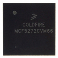
MCF5272CVM66 Freescale Semiconductor, MCF5272CVM66 Datasheet - Page 288

MCF5272CVM66
Manufacturer Part Number
MCF5272CVM66
Description
IC MPU 66MHZ COLDFIRE 196-MAPBGA
Manufacturer
Freescale Semiconductor
Series
MCF527xr
Specifications of MCF5272CVM66
Core Processor
Coldfire V2
Core Size
32-Bit
Speed
66MHz
Connectivity
EBI/EMI, Ethernet, I²C, SPI, UART/USART, USB
Peripherals
DMA, WDT
Number Of I /o
32
Program Memory Size
16KB (4K x 32)
Program Memory Type
ROM
Ram Size
1K x 32
Voltage - Supply (vcc/vdd)
3 V ~ 3.6 V
Oscillator Type
External
Operating Temperature
-40°C ~ 85°C
Package / Case
196-MAPBGA
Cpu Speed
66MHz
Embedded Interface Type
UART, QSPI, USB, TDM
Digital Ic Case Style
BGA
No. Of Pins
196
Supply Voltage Range
3V To 3.6V
Rohs Compliant
Yes
Family Name
MCF5xxx
Device Core
ColdFire
Device Core Size
32b
Frequency (max)
66MHz
Instruction Set Architecture
RISC
Supply Voltage 1 (typ)
3.3V
Operating Temp Range
-40C to 85C
Operating Temperature Classification
Industrial
Mounting
Surface Mount
Pin Count
196
Package Type
MA-BGA
Lead Free Status / RoHS Status
Lead free / RoHS Compliant
Eeprom Size
-
Data Converters
-
Lead Free Status / Rohs Status
Compliant
Available stocks
Company
Part Number
Manufacturer
Quantity
Price
Company:
Part Number:
MCF5272CVM66
Manufacturer:
MOT
Quantity:
3
Company:
Part Number:
MCF5272CVM66
Manufacturer:
Freescale Semiconductor
Quantity:
10 000
Part Number:
MCF5272CVM66
Manufacturer:
FREESCALE
Quantity:
20 000
Company:
Part Number:
MCF5272CVM66J
Manufacturer:
NSC
Quantity:
36
Company:
Part Number:
MCF5272CVM66J
Manufacturer:
Freescale Semiconductor
Quantity:
10 000
- Current page: 288 of 544
- Download datasheet (7Mb)
Universal Serial Bus (USB)
12.3.4
The access times for the USB module depend on whether the access is to a register, to an endpoint FIFO
(EPnDR register), or to the configuration RAM.
12.3.4.1
The USB module registers are accessed through the internal S-bus. Each register access takes 3 clock
cycles for reads and writes.
12.3.4.2
The FIFO access time depends on the size, the time between accesses, and whether the previous FIFO
access was for the same endpoint. After a longword access to an endpoint’s FIFO, the next longword in
the FIFO is cached for a quicker access time on the next longword read. This mechanism is reset every
time another endpoint is accessed.
12.3.4.3
The configuration RAM is longword accessible only. Access times for reads from the configuration RAM
are eight clock cycles per access. Clock cycle access times for back-to-back writes to the configuration
RAM are 3-5-5-5-5-5... Access times for writes separated by at least 1 clock cycle are 3-3-3-3-3-3…
12-30
9. Interface #0 Descriptor
10. Endpoint #1 Descriptor
11. Configuration #3 Descriptor
12. Interface #0 Descriptor
13. Endpoint #1 Descriptor
14. Endpoint #2 Descriptor
USB Module Access Times
Registers
Endpoint FIFOs
Configuration RAM
Byte
Word
Long (back to back)
Long (1 clock gap)
Long (2 clock gap)
Long (3+ clock gap)
MCF5272 ColdFire
Access Type
Table 12-19. USB FIFO Access Timing
Table 12-19
®
Integrated Microprocessor User’s Manual, Rev. 3
5
6
8-4-6-6-6-6...
8-3-5-5-5-5...
8-3-4-4-4-4...
8-3-3-3-3-3...
shows the access times for the FIFOs.
Read
4
4
4-6-6-6-6-6...
4-5-5-5-5-5...
4-4-4-4-4-4...
4-4-4-4-4-4...
Write
Freescale Semiconductor
Related parts for MCF5272CVM66
Image
Part Number
Description
Manufacturer
Datasheet
Request
R
Part Number:
Description:
Mcf5272 Coldfire Integrated Microprocessor User
Manufacturer:
Freescale Semiconductor, Inc
Datasheet:

Part Number:
Description:
MCF5272 Interrupt Service Routine for the Physical Layer Interface Controller
Manufacturer:
Freescale Semiconductor / Motorola
Datasheet:
Part Number:
Description:
Manufacturer:
Freescale Semiconductor, Inc
Datasheet:
Part Number:
Description:
Manufacturer:
Freescale Semiconductor, Inc
Datasheet:
Part Number:
Description:
Manufacturer:
Freescale Semiconductor, Inc
Datasheet:
Part Number:
Description:
Manufacturer:
Freescale Semiconductor, Inc
Datasheet:
Part Number:
Description:
Manufacturer:
Freescale Semiconductor, Inc
Datasheet:
Part Number:
Description:
Manufacturer:
Freescale Semiconductor, Inc
Datasheet:
Part Number:
Description:
Manufacturer:
Freescale Semiconductor, Inc
Datasheet:
Part Number:
Description:
Manufacturer:
Freescale Semiconductor, Inc
Datasheet:
Part Number:
Description:
Manufacturer:
Freescale Semiconductor, Inc
Datasheet:
Part Number:
Description:
Manufacturer:
Freescale Semiconductor, Inc
Datasheet:
Part Number:
Description:
Manufacturer:
Freescale Semiconductor, Inc
Datasheet:
Part Number:
Description:
Manufacturer:
Freescale Semiconductor, Inc
Datasheet:
Part Number:
Description:
Manufacturer:
Freescale Semiconductor, Inc
Datasheet:


