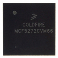
MCF5272CVM66 Freescale Semiconductor, MCF5272CVM66 Datasheet - Page 444

MCF5272CVM66
Manufacturer Part Number
MCF5272CVM66
Description
IC MPU 66MHZ COLDFIRE 196-MAPBGA
Manufacturer
Freescale Semiconductor
Series
MCF527xr
Specifications of MCF5272CVM66
Core Processor
Coldfire V2
Core Size
32-Bit
Speed
66MHz
Connectivity
EBI/EMI, Ethernet, I²C, SPI, UART/USART, USB
Peripherals
DMA, WDT
Number Of I /o
32
Program Memory Size
16KB (4K x 32)
Program Memory Type
ROM
Ram Size
1K x 32
Voltage - Supply (vcc/vdd)
3 V ~ 3.6 V
Oscillator Type
External
Operating Temperature
-40°C ~ 85°C
Package / Case
196-MAPBGA
Cpu Speed
66MHz
Embedded Interface Type
UART, QSPI, USB, TDM
Digital Ic Case Style
BGA
No. Of Pins
196
Supply Voltage Range
3V To 3.6V
Rohs Compliant
Yes
Family Name
MCF5xxx
Device Core
ColdFire
Device Core Size
32b
Frequency (max)
66MHz
Instruction Set Architecture
RISC
Supply Voltage 1 (typ)
3.3V
Operating Temp Range
-40C to 85C
Operating Temperature Classification
Industrial
Mounting
Surface Mount
Pin Count
196
Package Type
MA-BGA
Lead Free Status / RoHS Status
Lead free / RoHS Compliant
Eeprom Size
-
Data Converters
-
Lead Free Status / Rohs Status
Compliant
Available stocks
Company
Part Number
Manufacturer
Quantity
Price
Company:
Part Number:
MCF5272CVM66
Manufacturer:
MOT
Quantity:
3
Company:
Part Number:
MCF5272CVM66
Manufacturer:
Freescale Semiconductor
Quantity:
10 000
Part Number:
MCF5272CVM66
Manufacturer:
FREESCALE
Quantity:
20 000
Company:
Part Number:
MCF5272CVM66J
Manufacturer:
NSC
Quantity:
36
Company:
Part Number:
MCF5272CVM66J
Manufacturer:
Freescale Semiconductor
Quantity:
10 000
- Current page: 444 of 544
- Download datasheet (7Mb)
Signal Descriptions
Port A mode: I/O pin PA15.
Special interrupt mode: The INT6 interrupt can be enabled independently of the pin being configured for
DGNT1 or PA15. This is particularly useful when configured for PA15 operation because INT6 can be
used to signal a change of data on the PAx pins.
19.16.3 GCI/IDL TDM Ports 2 and 3
Physical Layer Interface port 2 is an additional GCI/IDL port. This Physical Layer Interface shares the
DIN1, DOUT1, and DCL1 pins of Physical Layer Interface port 1. The operating mode is selected by the
same register control bit that selects the operating mode for port 1.
Physical Layer Interface port 3 is an additional GCI/IDL port. This Physical Layer Interface shares the
DIN1, DOUT1, and DCL1 pins of Physical Layer Interface port 1. The operating mode is selected by the
same register control bit that selects the operating mode for port 1.
Port 3 can also have its input and output signals redirected to DIN3 and DOUT3 respectively.
19.16.3.1 GCI/IDL Delayed Frame Sync 2 (DFSC2/PA12)
IDL/GCI Modes: DFSC2 is used as a programmable delayed frame sync for external IDL/GCI devices that
use port 2 but are connected to the port 1 data pins. Port 2 uses the DFSC2 frame sync internally to ensure
alignment with external devices synchronized with DFSC2. The width of this signal can be configured for
1, 2, 8, or 16 DCL clocks duration. The location of this frame sync is programmable in single clock
increments up to a maximum count of 0x3FF.
Port A mode: I/O pin PA12.
19.16.3.2 GCI/IDL Delayed Frame Sync 3 (DFSC3/PA13)
Output pin DFSC3. This active high signal is used as a programmable delayed frame sync for external
IDL/GCI devices that use port 3 but are connected to the port 1 or port 3 data pins. Port 3 uses the DFSC3
frame sync internally to ensure alignment with external devices synchronized with DFSC3. The width of
this signal can be configured for 1, 2, 8, or 16 DCL clocks duration. The location of this frame sync is
programmable in single clock increments up to a maximum count of 0x3FF.
Port A mode: I/O pin PA13.
19.16.3.3 QSPI_CS3, Port 3 GCI/IDL Data Out 3, PA7 (PA7/DOUT3/QSPI_CS3)
QSPI mode: The QSPI chip select, QSPI_CS3, is the default configuration after device reset. QSPI_CS3
can be programmed to be active high or low.
IDL mode: This pin can be configured as a dedicated output for clocking data out of IDL port 3. Data is
clocked out of DOUT3 on the rising edge of DCL1. After device reset port 3 is connected to DOUT1 by
setting a bit in the PLIC module configuration register, this pin can be configured as a dedicated output for
IDL/GCI port 3.
®
MCF5272 ColdFire
Integrated Microprocessor User’s Manual, Rev. 3
19-34
Freescale Semiconductor
Related parts for MCF5272CVM66
Image
Part Number
Description
Manufacturer
Datasheet
Request
R
Part Number:
Description:
Mcf5272 Coldfire Integrated Microprocessor User
Manufacturer:
Freescale Semiconductor, Inc
Datasheet:

Part Number:
Description:
MCF5272 Interrupt Service Routine for the Physical Layer Interface Controller
Manufacturer:
Freescale Semiconductor / Motorola
Datasheet:
Part Number:
Description:
Manufacturer:
Freescale Semiconductor, Inc
Datasheet:
Part Number:
Description:
Manufacturer:
Freescale Semiconductor, Inc
Datasheet:
Part Number:
Description:
Manufacturer:
Freescale Semiconductor, Inc
Datasheet:
Part Number:
Description:
Manufacturer:
Freescale Semiconductor, Inc
Datasheet:
Part Number:
Description:
Manufacturer:
Freescale Semiconductor, Inc
Datasheet:
Part Number:
Description:
Manufacturer:
Freescale Semiconductor, Inc
Datasheet:
Part Number:
Description:
Manufacturer:
Freescale Semiconductor, Inc
Datasheet:
Part Number:
Description:
Manufacturer:
Freescale Semiconductor, Inc
Datasheet:
Part Number:
Description:
Manufacturer:
Freescale Semiconductor, Inc
Datasheet:
Part Number:
Description:
Manufacturer:
Freescale Semiconductor, Inc
Datasheet:
Part Number:
Description:
Manufacturer:
Freescale Semiconductor, Inc
Datasheet:
Part Number:
Description:
Manufacturer:
Freescale Semiconductor, Inc
Datasheet:
Part Number:
Description:
Manufacturer:
Freescale Semiconductor, Inc
Datasheet:


