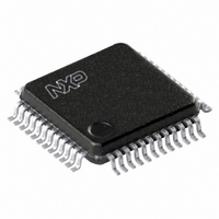
SC68C652BIB48,157 NXP Semiconductors, SC68C652BIB48,157 Datasheet - Page 11

SC68C652BIB48,157
Manufacturer Part Number
SC68C652BIB48,157
Description
IC UART DUAL 48LQFP
Manufacturer
NXP Semiconductors
Datasheet
1.SC68C652BIB48128.pdf
(43 pages)
Specifications of SC68C652BIB48,157
Features
2 Channels
Number Of Channels
2, DUART
Fifo's
32 Byte
Voltage - Supply
2.5V, 3.3V, 5V
With Auto Flow Control
Yes
With Irda Encoder/decoder
Yes
With False Start Bit Detection
Yes
With Modem Control
Yes
Mounting Type
Surface Mount
Package / Case
48-LFQFP
Voltage
2.25 V ~ 5.5 V
Lead Free Status / RoHS Status
Lead free / RoHS Compliant
Other names
935278766157
SC68C652BIB48
SC68C652BIB48
SC68C652BIB48
SC68C652BIB48
Available stocks
Company
Part Number
Manufacturer
Quantity
Price
Company:
Part Number:
SC68C652BIB48,157
Manufacturer:
NXP Semiconductors
Quantity:
10 000
NXP Semiconductors
SC68C652B_2
Product data sheet
6.6 Special feature software flow control
6.7 Hardware/software and time-out interrupts
as received data passes the programmed trigger level. To clear this condition, the
SC68C652B will transmit the programmed Xon1/Xon2 characters as soon as receive data
drops below the programmed trigger level.
A special feature is provided to detect an 8-bit character when EFR[5] is set. When 8-bit
character is detected, wit will be placed on the user-accessible data stack along with
normal incoming receive data. This condition is selected in conjunction with EFR[3:0].
Note that software flow control should be turned off when using this special mode by
setting EFR[3:0] to a logic 0.
The SC68C652B compares each incoming receive character with Xoff2 data. If a match
exists, the received data will be transferred to the FIFO, and ISR[4] will be set to indicate
detection of a special character. Although
each X-register with eight bits of character information, the actual number of bits is
dependent on the programmed word length. Line Control Register bits LCR[1:0] define the
number of character bits, that is, either 5 bits, 6 bits, 7 bits or 8 bits. The word length
selected by LCR[1:0] also determine the number of bits that will be used for the special
character comparison. Bit 0 in the X-registers corresponds with the LSB bit for the receive
character.
The interrupts are enabled by IER[3:0]. Care must be taken when handling these
interrupts. Following a reset, if Interrupt Enable Register (IER) bit 1 = 1, the SC68C652B
will issue a Transmit Holding Register interrupt. This interrupt must be serviced prior to
continuing operations. The ISR register provides the current singular highest priority
interrupt only. It could be noted that CTS and RTS interrupts have lowest interrupt priority.
A condition can exist where a higher priority interrupt may mask the lower priority
CTS/RTS interrupt(s). Only after servicing the higher pending interrupt will the lower
priority CTS/RTS interrupt(s) be reflected in the status register. Servicing the interrupt
without investigating further interrupt conditions can result in data errors.
When two interrupt conditions have the same priority, it is important to service these
interrupts correctly. Receive Data Ready and Receive Time-Out have the same interrupt
priority (when enabled by IER[0]). The receiver issues an interrupt after the number of
characters have reached the programmed trigger level. In this case, the SC68C652B
FIFO may hold more characters than the programmed trigger level. Following the removal
of a data byte, the user should re-check LSR[0] for additional characters. A Receive
Time-Out will not occur if the receive FIFO is empty. The time-out counter is reset at the
center of each stop bit received or each time the receive holding register (RHR) is read.
The actual time-out value is 4 character time, including data information length, start bit,
parity bit, and the size of stop bit, that is, 1 , 1.5 , or 2 bit times.
Rev. 02 — 2 November 2009
Dual UART with 32-byte FIFOs and IrDA encoder/decoder
Table 9 “SC68C652B internal registers”
SC68C652B
© NXP B.V. 2009. All rights reserved.
shows
11 of 43


