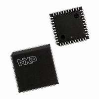
SC28L91A1A,512 NXP Semiconductors, SC28L91A1A,512 Datasheet - Page 29

SC28L91A1A,512
Manufacturer Part Number
SC28L91A1A,512
Description
IC UART SINGLE W/FIFO 44-PLCC
Manufacturer
NXP Semiconductors
Series
IMPACTr
Datasheet
1.SC28L91A1A529.pdf
(43 pages)
Specifications of SC28L91A1A,512
Features
False-start Bit Detection
Number Of Channels
1, UART
Fifo's
16 Byte
Voltage - Supply
3.3V, 5V
With Auto Flow Control
Yes
With False Start Bit Detection
Yes
With Modem Control
Yes
With Cmos
Yes
Mounting Type
Surface Mount
Package / Case
44-PLCC
Voltage
3 V ~ 3.6 V, 4.5 V ~ 5.5 V
Lead Free Status / RoHS Status
Lead free / RoHS Compliant
Other names
935267418512
SC28L91A1A
SC28L91A1A
SC28L91A1A
SC28L91A1A
Available stocks
Company
Part Number
Manufacturer
Quantity
Price
Company:
Part Number:
SC28L91A1A,512
Manufacturer:
NXP Semiconductors
Quantity:
10 000
Philips Semiconductors
OPCR Output Port Configuration Register
OPCR[7]—OP7 Output Select
This bit programs the OP7 output to provide one of the following:
OPCR[6]—OP6 Output Select
This bit programs the OP6 output to provide one of the following:
OPCR[5]—OP5 Output Select
This bit programs the OP5 output to provide one of the following:
OPCR[4]—OP4 Output Select
This field programs the OP4 output to provide one of the following:
SOPR—Set the Output Port Bits (OPR)
SOPR[7:0]—Ones in the byte written to this register will cause the corresponding bit positions in the OPR to set to 1. Zeros have no effect. This
allows software to set individual bits with our keeping a copy of the OPR bit configuration.
ROPR—Reset Output Port Bits (OPR)
ROPR[7:0]—Ones in the byte written to the ROPR will cause the corresponding bit positions in the OPR to set to 0. Zeros have no effect. This
allows software to reset individual bits with our keeping a copy of the OPR bit configuration.
2004 Oct 21
Addr
OPCR
0x0D
0
1
0
1
0
1
0
1
Addr
SOPR
0x0E
Addr
ROPR
0x0F
3.3 V or 5.0 V Universal Asynchronous
Receiver/Transmitter (UART)
The complement of OPR[7].
reserved
The complement of OPR[6].
The transmitter interrupt output which is the complement of
ISR[0]. When in this mode OP6 acts as an open-drain out-
put. Note that this output is not masked by the contents of
the IMR.
The complement of OPR[5].
Reserved
The complement of OPR[4].
The receiver interrupt output which is the complement of
ISR[1]. When in this mode OP4 acts as an open-drain out-
put. Note that this output is not masked by the contents of
the IMR.
Bit 7
OP 7
1 = set bit
0 = no change
Bit 7
OP 7
1 = reset bit
0 = no change
Bit 7
OP7
0 = OPR[7]
1 = Reserved
BIT 6
OP 6
1 = set bit
0 = no change
BIT 6
OP 6
1 = reset bit
0 = no change
BIT 6
OP6
0 = OPR[6]
1 = TxRDY
BIT 5
OP 5
1 = set bit
0 = no change
BIT 5
OP 5
1 = reset bit
0 = no change
BIT 5
OP5
0 = OPR[5]
1 = Reserved
BIT 4
OP 4
1 = set bit
0 = no change
BIT 4
OP 4
1 = reset bit
0 = no change
29
BIT 4
OP4
0 = OPR[4]
1 = RxRDY/FFULL
OPCR[3:2]—OP3 Output Select
This bit programs the OP3 output to provide one of the following:
OPCR[1:0]—OP2 Output Select
This field programs the OP2 output to provide one of the following:
00
01
10
11
00
01
10
11
BIT 3
OP 3
1 = set bit
0 = no change
BIT 3
OP 3
1 = reset bit
0 = no change
The 1X clock for the receiver, which is the clock that samples
The complement of OPR[3].
The counter/timer output, in which case OP3 acts as an
open-drain output. In the timer mode, this output is a square
wave at the programmed frequency. In the counter mode,
the output remains High until terminal count is reached, at
which time it goes Low. The output returns to the High state
when the counter is stopped by a stop counter command.
Note that this output is not masked by the contents of the
IMR.
Reserved
Reserved
The complement of OPR[2].
The 16X clock for the transmitter. This is the clock selected
by CSR[3:0], and will be a 1X clock if CSR[3:0] = 1111.
The 1X clock for the transmitter, which is the clock that shifts
the transmitted data. If data is not being transmitted, a free
running 1X clock is output.
the received data. If data is not being received, a free run-
ning 1X clock is output.
BIT 3
OP3
00 = OPR[3]
01 = C/T OUTPUT
10 = Reserved
11 = Reserved
BIT 2
OP 2
1 = set bit
0 = no change
BIT 2
OP 2
1 = reset bit
0 = no change
BIT 2
OP2
BIT 1
OP 1
1 = set bit
0 = no change
BIT 1
OP 1
1 = reset bit
0 = no change
BIT 1
OP1
00 = OPR[2]
01 = TxC(16X)
10 = TxC(1X)
11 = RxC(1X)
SC28L91
Product data sheet
BIT 0
OP 0
1 = set bit
0 = no change
BIT 0
OP 0
1 = reset bit
0 = no change
BIT 0
OP0


