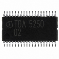
TDA5250 Infineon Technologies, TDA5250 Datasheet - Page 25

TDA5250
Manufacturer Part Number
TDA5250
Description
TX/RX ASK/FSK 868-870MHZ 38TSSOP
Manufacturer
Infineon Technologies
Type
Transceiverr
Specifications of TDA5250
Package / Case
38-TSSOP
Frequency
868MHz
Data Rate - Maximum
64kbps
Modulation Or Protocol
ASK, FSK
Applications
RKE, Remote Control Systems
Power - Output
9dBm
Sensitivity
-109dBm
Voltage - Supply
2.1 V ~ 5.5 V
Current - Receiving
9mA
Current - Transmitting
12mA
Data Interface
PCB, Surface Mount
Antenna Connector
PCB, Surface Mount
Operating Temperature
-40°C ~ 85°C
Operating Frequency
870 MHz
Operating Supply Voltage
2.5 V, 3.3 V, 5 V
Maximum Operating Temperature
+ 85 C
Minimum Operating Temperature
- 40 C
Mounting Style
SMD/SMT
Operating Temperature (min)
-40C
Operating Temperature (max)
85C
Operating Temperature Classification
Industrial
Product Depth (mm)
4.4mm
Product Length (mm)
9.7mm
Operating Supply Voltage (min)
2.1V
Operating Supply Voltage (max)
5.5V
Lead Free Status / RoHS Status
Lead free / RoHS Compliant
Memory Size
-
Lead Free Status / Rohs Status
Compliant
Other names
SP000012956
TDA5250
TDA5250INTR
TDA5250XT
TDA5250XT
TDA5250
TDA5250INTR
TDA5250XT
TDA5250XT
Available stocks
Company
Part Number
Manufacturer
Quantity
Price
Company:
Part Number:
TDA5250
Manufacturer:
Infineon Technologies
Quantity:
135
Company:
Part Number:
TDA5250D2
Manufacturer:
INFINEON
Quantity:
300
Part Number:
TDA5250D2
Manufacturer:
INFINEON/英飞凌
Quantity:
20 000
Table 2-7
Data Transition:
Data transition on the pin BusData can only occur when BusCLK is LOW. BusData transitions while
BusCLK is HIGH will be interpreted as start or stop condition.
Start Condition (STA):
A start condition is defined by a HIGH to LOW transition of the BusData line while BusCLK is HIGH.
This start condition must precede any command and initiate a data transfer onto the bus.
Stop Condition (STO):
A stop condition is defined by a LOW to HIGH transition of the BusData line while BusCLK is HIGH.
This condition terminates the communication between the devices and forces the bus interface into
the initial state.
Acknowledge (ACK):
Indicates a successful data transfer. The transmitter will release the bus after sending 8 bit of data.
During the 9th clock cycle the receiver will set the SDA line to LOW level to indicate it has received
the 8 bits of data correctly.
Data Transfer Write Mode:
To start the communication, the bus master must initiate a start condition (STA), followed by the 8bit
chip address. The chip address for the TDA5250 is fixed as „1110000“ (MSB at first). The last bit
(LSB=A0) of the chip address byte defines the type of operation to be performed:
A0=0, a write operation is selected and A0=1 a read operation is selected.
After this comparison the TDA5250 will generate an ACK and awaits the desired sub address byte
(00H...0FH) and data bytes. At the end of the data transition the master has to generate the stop
condition (STO).
Data Transfer Read Mode:
To start the communication in the read mode, the bus master must initiate a start condition (STA),
followed by the 8 bit chip address (write: A0=0), followed by the sub address to read (80H, 81H),
followed by the chip address (read: A0=1). After that procedure the data of the selected register
(80H, 81H) is read out. During this time the data line has to be kept in HIGH state and the chip sends
out the data. At the end of data transition the master has to generate the stop condition (STO).
Bus Data Format in I
Data Sheet
MSB
1
1
1
1
Chip address Organization
1
1
2
0
0
C Mode
0
0
0
0
0
0
25
LSB
0
1
Chip Address Write
Chip Address Read
Functional Description
Function
TDA5250 D2
Version 1.7
2007-02-26


