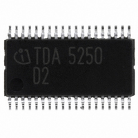
TDA5250 Infineon Technologies, TDA5250 Datasheet - Page 44

TDA5250
Manufacturer Part Number
TDA5250
Description
TX/RX ASK/FSK 868-870MHZ 38TSSOP
Manufacturer
Infineon Technologies
Type
Transceiverr
Specifications of TDA5250
Package / Case
38-TSSOP
Frequency
868MHz
Data Rate - Maximum
64kbps
Modulation Or Protocol
ASK, FSK
Applications
RKE, Remote Control Systems
Power - Output
9dBm
Sensitivity
-109dBm
Voltage - Supply
2.1 V ~ 5.5 V
Current - Receiving
9mA
Current - Transmitting
12mA
Data Interface
PCB, Surface Mount
Antenna Connector
PCB, Surface Mount
Operating Temperature
-40°C ~ 85°C
Operating Frequency
870 MHz
Operating Supply Voltage
2.5 V, 3.3 V, 5 V
Maximum Operating Temperature
+ 85 C
Minimum Operating Temperature
- 40 C
Mounting Style
SMD/SMT
Operating Temperature (min)
-40C
Operating Temperature (max)
85C
Operating Temperature Classification
Industrial
Product Depth (mm)
4.4mm
Product Length (mm)
9.7mm
Operating Supply Voltage (min)
2.1V
Operating Supply Voltage (max)
5.5V
Lead Free Status / RoHS Status
Lead free / RoHS Compliant
Memory Size
-
Lead Free Status / Rohs Status
Compliant
Other names
SP000012956
TDA5250
TDA5250INTR
TDA5250XT
TDA5250XT
TDA5250
TDA5250INTR
TDA5250XT
TDA5250XT
Available stocks
Company
Part Number
Manufacturer
Quantity
Price
Company:
Part Number:
TDA5250
Manufacturer:
Infineon Technologies
Quantity:
135
Company:
Part Number:
TDA5250D2
Manufacturer:
INFINEON
Quantity:
300
Part Number:
TDA5250D2
Manufacturer:
INFINEON/英飞凌
Quantity:
20 000
3.1.4
The power amplifier operates in a high efficient class C mode. This mode is characterized by a
pulsed operation of the power amplifier transistor at a current flow angle of θ<<π. A frequency
selective network at the amplifier output passes the fundamental frequency component of the pulse
spectrum of the collector current to the load. The load and its resonance transformation to the
collector of the power amplifier can be generalized by the equivalent circuit of Figure 3-6. The tank
circuit L//C//RL in parallel to the output impedance of the transistor should be in resonance at the
operating frequency of the transmitter.
Figure 3-6
The optimum load at the collector of the power amplifier for “critical” operation under idealized
conditions at resonance is:
A typical value of R LC for an RF output power of P o = 13mW is:
Critical” operation is characterized by the RF peak voltage swing at the collector of the PA transistor
to just reach the supply voltage V
explained by the low power loss at the transistor.
During the conducting phase of the transistor there is no or only a very small collector voltage
present, thus minimizing the power loss of the transistor (i
current flow angles of θ<<π
parasitics will reduce the “critical” R
The output power P o will be reduced when operating in an “overcritical” mode at a R
shown in Figure 3-7, however, power efficiency E (and bandwidth) will increase by some degree
when operating at higher R L . The collector efficiency E is defined as
Data Sheet
R
R
LC
LC
=
Power-Amplifier
=
2
V
Equivalent power amplifier tank circuit
2
P
S
O
∗
2
. 0
3
2
013
=
350
.
In practice the RF-saturation voltage of the PA transistor and other
Ω
S
. The high efficiency under “critical” operating conditions can be
LC
L
.
C
44
R
V
L
S
C
*u
CE
). This is particularly true for low
[3 – 8]
[3 – 9]
TDA5250 D2
Version 1.7
Equivalent_power_wmf.
Application
L
2007-02-26
> R
LC
. As


