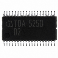
TDA5250 Infineon Technologies, TDA5250 Datasheet - Page 69

TDA5250
Manufacturer Part Number
TDA5250
Description
TX/RX ASK/FSK 868-870MHZ 38TSSOP
Manufacturer
Infineon Technologies
Type
Transceiverr
Specifications of TDA5250
Package / Case
38-TSSOP
Frequency
868MHz
Data Rate - Maximum
64kbps
Modulation Or Protocol
ASK, FSK
Applications
RKE, Remote Control Systems
Power - Output
9dBm
Sensitivity
-109dBm
Voltage - Supply
2.1 V ~ 5.5 V
Current - Receiving
9mA
Current - Transmitting
12mA
Data Interface
PCB, Surface Mount
Antenna Connector
PCB, Surface Mount
Operating Temperature
-40°C ~ 85°C
Operating Frequency
870 MHz
Operating Supply Voltage
2.5 V, 3.3 V, 5 V
Maximum Operating Temperature
+ 85 C
Minimum Operating Temperature
- 40 C
Mounting Style
SMD/SMT
Operating Temperature (min)
-40C
Operating Temperature (max)
85C
Operating Temperature Classification
Industrial
Product Depth (mm)
4.4mm
Product Length (mm)
9.7mm
Operating Supply Voltage (min)
2.1V
Operating Supply Voltage (max)
5.5V
Lead Free Status / RoHS Status
Lead free / RoHS Compliant
Memory Size
-
Lead Free Status / Rohs Status
Compliant
Other names
SP000012956
TDA5250
TDA5250INTR
TDA5250XT
TDA5250XT
TDA5250
TDA5250INTR
TDA5250XT
TDA5250XT
Available stocks
Company
Part Number
Manufacturer
Quantity
Price
Company:
Part Number:
TDA5250
Manufacturer:
Infineon Technologies
Quantity:
135
Company:
Part Number:
TDA5250D2
Manufacturer:
INFINEON
Quantity:
300
Part Number:
TDA5250D2
Manufacturer:
INFINEON/英飞凌
Quantity:
20 000
Timing for data detection looks like the following. Two settings are possible: „Continuous“ and
„Single Shot“, which can be set by D5 and D6 in register 00H.
Figure 3-31
Note 1: Chip internal signal „Sequencer enables data detection“ has a LOW to HIGH transition
about 2.6ms after RX is activated (see Figure 2-15).
Note 2: The positive edge of the „Window Count Complete“ signal latches the result of comparison
of the analog to digital converted RSSI voltage with TH3 (register 08H). A logic combination of this
output and the result of the comparison with single/double TH x defines the internal signal
„data_valid“.
Figure 3-31 shows that the logic is ready for the next conversion after 3 periods of the data signal.
Timing in Single Shot mode can be seen in the subsequent figure:
Figure 3-32
Data Sheet
Frequency Detection timing in continuous mode
Frequency Detection timing in Single Shot mode
Compare with double
(Frequency) Window
Compare with single
Sequenzer enables
TH and latch result
TH and latch result
Compare with double
(Frequency) Window
Compare with single
Sequenzer enables
TH and latch result
TH and latch result
Count Complete
Counter Reset
data detection
Count Complete
Counter Reset
data detection
Gate time
Gate time
Data
start of conversion
Data
start of conversion
reset
reset
no possible start of next conversion
count
because of Single Shot Mode
69
comp.
count
possible start of next conversion
comp.
comp.
ready*
comp.
ready*
reset
count
t
t
t
t
t
t
t
Frequ_Detect_Timing_singleShot_wmf
Frequ_Detect_Timing_continuous.wmf
comp.
t
t
t
t
t
t
t
TDA5250 D2
Version 1.7
Application
2007-02-26


