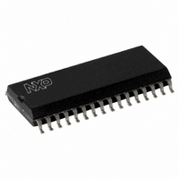
MFRC53101T/0FE,112 NXP Semiconductors, MFRC53101T/0FE,112 Datasheet - Page 17

MFRC53101T/0FE,112
Manufacturer Part Number
MFRC53101T/0FE,112
Description
IC MIFARE HS READER 32-SOIC
Manufacturer
NXP Semiconductors
Series
MIFARE®r
Specifications of MFRC53101T/0FE,112
Rf Type
Read Only
Frequency
13.56MHz
Features
ISO14443-A, ISO14443-B, ISO15693
Package / Case
32-SOIC (0.300", 7.50mm Width)
Product
RFID Readers
Operating Temperature Range
- 25 C to + 85 C
Lead Free Status / RoHS Status
Lead free / RoHS Compliant
Lead Free Status / RoHS Status
Lead free / RoHS Compliant, Lead free / RoHS Compliant
Other names
568-2224-5
935269691112
MFRC531
MFRC53101TD
935269691112
MFRC531
MFRC53101TD
Available stocks
Company
Part Number
Manufacturer
Quantity
Price
Part Number:
MFRC53101T/0FE,112
Manufacturer:
NXP/恩智浦
Quantity:
20 000
NXP Semiconductors
MFRC531_34
Product data sheet
PUBLIC
9.2.3.2 Storage of keys in the EEPROM
9.3.1.1 Access rules
9.3.1 Accessing the FIFO buffer
9.3 FIFO buffer
Remark: It is possible to load data for other key formats into the EEPROM key storage
location. However, it is not possible to validate card authentication with data which will
cause the LoadKeyE2 command (see
The MFRC531 reserves 384 bytes of memory in the EEPROM for the Crypto1 keys. No
memory segmentation is used to mirror the 12-byte structure of key storage. Thus, every
byte of the dedicated memory area can be the start of a key.
Example: If the key loading cycle starts at the last byte address of an EEPROM block, (for
example, key byte 0 is stored at 12Fh), the next bytes are stored in the next EEPROM
block, for example, key byte 1 is stored at 130h, byte 2 at 131h up to byte 11 at 13Ah.
Based on the 384 bytes of memory and a single key needing 12 bytes, then up to 32
different keys can be stored in the EEPROM.
Remark: It is not possible to load a key exceeding the EEPROM byte location 1FFh.
An 8 × 64 bit FIFO buffer is used in the MFRC531 to act as a parallel-to-parallel converter.
It buffers both the input and output data streams between the microprocessor and the
internal circuitry of the MFRC531. This makes it possible to manage data streams up to
64 bytes long without needing to take timing constraints into account.
The FIFO buffer input and output data bus is connected to the FIFOData register. Writing
to this register stores one byte in the FIFO buffer and increments the FIFO buffer write
pointer. Reading from this register shows the FIFO buffer contents stored at the FIFO
buffer read pointer and increments the FIFO buffer read pointer. The distance between the
write and read pointer can be obtained by reading the FIFOLength register.
When the microprocessor starts a command, the MFRC531 can still access the FIFO
buffer while the command is running. Only one FIFO buffer has been implemented which
is used for input and output. Therefore, the microprocessor must ensure that there are no
inadvertent FIFO buffer accesses.
during command processing.
Table 17.
Active
command
StartUp
Idle
Transmit
Receive
Transceive
WriteE2
FIFO buffer access
FIFO buffer
μp Write
-
-
yes
-
yes
yes
Rev. 3.4 — 26 January 2010
μp Read
-
-
-
yes
yes
-
056634
Table 17
Section 11.6.1 on page
Remark
the microprocessor has to know the state of the
command (transmitting or receiving)
gives an overview of FIFO buffer access
88) to fail.
ISO/IEC 14443 reader IC
MFRC531
© NXP B.V. 2010. All rights reserved.
17 of 116


