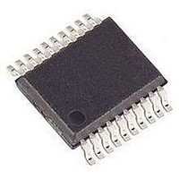
PIC16F1828-I/SS Microchip Technology, PIC16F1828-I/SS Datasheet - Page 163

PIC16F1828-I/SS
Manufacturer Part Number
PIC16F1828-I/SS
Description
IC PIC MCU 8BIT 14KB FLSH 20SSOP
Manufacturer
Microchip Technology
Series
PIC® XLP™ 16Fr
Datasheets
1.PIC16F722-ISS.pdf
(8 pages)
2.PIC16F1826-IP.pdf
(40 pages)
3.PIC16F1824-ISL.pdf
(2 pages)
4.PIC16F1824-ISL.pdf
(419 pages)
5.PIC16F1824-ISL.pdf
(10 pages)
Specifications of PIC16F1828-I/SS
Core Size
8-Bit
Program Memory Size
7KB (4K x 14)
Core Processor
PIC
Speed
32MHz
Connectivity
I²C, SPI, UART/USART
Peripherals
Brown-out Detect/Reset, POR, PWM, WDT
Number Of I /o
17
Program Memory Type
FLASH
Eeprom Size
256 x 8
Ram Size
256 x 8
Voltage - Supply (vcc/vdd)
1.8 V ~ 5.5 V
Data Converters
A/D 12x10b
Oscillator Type
Internal
Operating Temperature
-40°C ~ 85°C
Package / Case
20-SSOP (0.200", 5.30mm Width)
Controller Family/series
PIC16F
No. Of I/o's
18
Eeprom Memory Size
256Byte
Ram Memory Size
256Byte
Cpu Speed
32MHz
No. Of Timers
5
Lead Free Status / RoHS Status
Lead free / RoHS Compliant
Available stocks
Company
Part Number
Manufacturer
Quantity
Price
Part Number:
PIC16F1828-I/SS
Manufacturer:
MIC
Quantity:
20 000
- PIC16F722-ISS PDF datasheet
- PIC16F1826-IP PDF datasheet #2
- PIC16F1824-ISL PDF datasheet #3
- PIC16F1824-ISL PDF datasheet #4
- PIC16F1824-ISL PDF datasheet #5
- Current page: 163 of 419
- Download datasheet (4Mb)
17.0
The Digital-to-Analog Converter supplies a variable
voltage reference, ratiometric with the input source,
with 32 selectable output levels.
The input of the DAC can be connected to:
• External V
• V
• FVR (Fixed Voltage Reference)
The output of the DAC can be configured to supply a
reference voltage to the following:
• Comparator positive input
• ADC input channel
• DACOUT pin
The Digital-to-Analog Converter (DAC) can be enabled
by setting the DACEN bit of the DACCON0 register.
17.1
The DAC has 32 voltage level ranges. The 32 levels
are set with the DACR<4:0> bits of the DACCON1
register.
The DAC output voltage is determined by the following
equations:
EQUATION 17-1:
17.2
The DAC output value is derived using a resistor ladder
with each end of the ladder tied to a positive and
negative voltage reference input source. If the voltage
of either input source fluctuates, a similar fluctuation will
result in the DAC output value.
The value of the individual resistors within the ladder
can
Specifications”.
2010 Microchip Technology Inc.
V
Note:
OUT
DD
=
supply voltage
be
DIGITAL-TO-ANALOG
CONVERTER (DAC) MODULE
Output Voltage Selection
Ratiometric Output Level
V
V
V
SOURCE
REF
found
SOURCE
REF
+. V
pins
+ V
SOURCE
+ can equal FVR Buffer 2, V
–
in
DAC OUTPUT VOLTAGE
SOURCE
- can equal V
Section 30.0
-
DACR<4:0>
------------------------------ -
2 5
SS
or V
“Electrical
REF
+ V
DD
-.
SRC
or
Preliminary
-
17.3
The DAC can be output to the DACOUT pin by setting
the DACOE bit of the DACCON0 register to ‘1’. Selecting
the DAC reference voltage for output on the DACOUT
pin automatically overrides the digital output buffer and
digital input threshold detector functions of that pin.
Reading the DACOUT pin when it has been configured
for DAC reference voltage output will always return a ‘0’.
Due to the limited current drive capability, a buffer must
be used on the DAC voltage reference output for
external connections to DACOUT.
an example buffering technique.
PIC16(L)F1824/1828
DAC Voltage Reference Output
Figure 17-2
DS41419B-page 163
shows
Related parts for PIC16F1828-I/SS
Image
Part Number
Description
Manufacturer
Datasheet
Request
R

Part Number:
Description:
IC, 8BIT MCU, PIC16F, 32MHZ, SOIC-18
Manufacturer:
Microchip Technology
Datasheet:

Part Number:
Description:
IC, 8BIT MCU, PIC16F, 32MHZ, SSOP-20
Manufacturer:
Microchip Technology
Datasheet:

Part Number:
Description:
IC, 8BIT MCU, PIC16F, 32MHZ, DIP-18
Manufacturer:
Microchip Technology
Datasheet:

Part Number:
Description:
IC, 8BIT MCU, PIC16F, 32MHZ, QFN-28
Manufacturer:
Microchip Technology
Datasheet:

Part Number:
Description:
IC, 8BIT MCU, PIC16F, 32MHZ, QFN-28
Manufacturer:
Microchip Technology
Datasheet:

Part Number:
Description:
IC, 8BIT MCU, PIC16F, 32MHZ, QFN-28
Manufacturer:
Microchip Technology
Datasheet:

Part Number:
Description:
IC, 8BIT MCU, PIC16F, 32MHZ, SSOP-20
Manufacturer:
Microchip Technology
Datasheet:

Part Number:
Description:
IC, 8BIT MCU, PIC16F, 20MHZ, DIP-40
Manufacturer:
Microchip Technology
Datasheet:

Part Number:
Description:
IC, 8BIT MCU, PIC16F, 32MHZ, QFN-28
Manufacturer:
Microchip Technology
Datasheet:

Part Number:
Description:
IC, 8BIT MCU, PIC16F, 20MHZ, MQFP-44
Manufacturer:
Microchip Technology
Datasheet:

Part Number:
Description:
IC, 8BIT MCU, PIC16F, 20MHZ, QFN-20
Manufacturer:
Microchip Technology
Datasheet:

Part Number:
Description:
IC, 8BIT MCU, PIC16F, 32MHZ, QFN-28
Manufacturer:
Microchip Technology
Datasheet:

Part Number:
Description:
MCU 14KB FLASH 768B RAM 64-TQFP
Manufacturer:
Microchip Technology
Datasheet:

Part Number:
Description:
7 KB Flash, 384 Bytes RAM, 32 MHz Int. Osc, 16 I/0, Enhanced Mid Range Core, Low
Manufacturer:
Microchip Technology

Part Number:
Description:
14KB Flash, 512B RAM, 256B EEPROM, LCD, 1.8-5.5V 40 UQFN 5x5x0.5mm TUBE
Manufacturer:
Microchip Technology
Datasheet:


