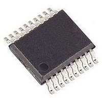
PIC16F1828-I/SS Microchip Technology, PIC16F1828-I/SS Datasheet - Page 50

PIC16F1828-I/SS
Manufacturer Part Number
PIC16F1828-I/SS
Description
IC PIC MCU 8BIT 14KB FLSH 20SSOP
Manufacturer
Microchip Technology
Series
PIC® XLP™ 16Fr
Datasheets
1.PIC16F722-ISS.pdf
(8 pages)
2.PIC16F1826-IP.pdf
(40 pages)
3.PIC16F1824-ISL.pdf
(2 pages)
4.PIC16F1824-ISL.pdf
(419 pages)
5.PIC16F1824-ISL.pdf
(10 pages)
Specifications of PIC16F1828-I/SS
Core Size
8-Bit
Program Memory Size
7KB (4K x 14)
Core Processor
PIC
Speed
32MHz
Connectivity
I²C, SPI, UART/USART
Peripherals
Brown-out Detect/Reset, POR, PWM, WDT
Number Of I /o
17
Program Memory Type
FLASH
Eeprom Size
256 x 8
Ram Size
256 x 8
Voltage - Supply (vcc/vdd)
1.8 V ~ 5.5 V
Data Converters
A/D 12x10b
Oscillator Type
Internal
Operating Temperature
-40°C ~ 85°C
Package / Case
20-SSOP (0.200", 5.30mm Width)
Controller Family/series
PIC16F
No. Of I/o's
18
Eeprom Memory Size
256Byte
Ram Memory Size
256Byte
Cpu Speed
32MHz
No. Of Timers
5
Lead Free Status / RoHS Status
Lead free / RoHS Compliant
Available stocks
Company
Part Number
Manufacturer
Quantity
Price
Part Number:
PIC16F1828-I/SS
Manufacturer:
MIC
Quantity:
20 000
- PIC16F722-ISS PDF datasheet
- PIC16F1826-IP PDF datasheet #2
- PIC16F1824-ISL PDF datasheet #3
- PIC16F1824-ISL PDF datasheet #4
- PIC16F1824-ISL PDF datasheet #5
- Current page: 50 of 419
- Download datasheet (4Mb)
PIC16(L)F1824/1828
3.5.2
The linear data memory is the region from FSR
address 0x2000 to FSR address 0x29AF. This region is
a virtual region that points back to the 80-byte blocks of
GPR memory in all the banks.
Unimplemented memory reads as 0x00. Use of the
linear data memory region allows buffers to be larger
than 80 bytes because incrementing the FSR beyond
one bank will go directly to the GPR memory of the next
bank.
The 16 bytes of common memory are not included in
the linear data memory region.
FIGURE 3-10:
DS41419B-page 50
7
0
0
FSRnH
1
Location Select
LINEAR DATA MEMORY
0
LINEAR DATA MEMORY
MAP
7
FSRnL
0x2000
0x29AF
Bank 30
Bank 0
0x06F
0x020
0x0A0
Bank 1
0x0EF
0x120
Bank 2
0xF20
0xF6F
0x16F
0
Preliminary
3.5.3
To make constant data access easier, the entire
program Flash memory is mapped to the upper half of
the FSR address space. When the MSB of FSRnH is
set, the lower 15 bits are the address in program
memory which will be accessed through INDF. Only the
lower 8 bits of each memory location is accessible via
INDF. Writing to the program Flash memory cannot be
accomplished
instructions that access program Flash memory via the
FSR/INDF interface will require one additional
instruction cycle to complete.
FIGURE 3-11:
7
1
FSRnH
Location Select
PROGRAM FLASH MEMORY
via
0
the
PROGRAM FLASH
MEMORY MAP
2010 Microchip Technology Inc.
7
FSR/INDF
FSRnL
0x8000
0xFFFF
interface.
Program
Flash
Memory
(low 8
bits)
0x0000
0x7FFF
0
All
Related parts for PIC16F1828-I/SS
Image
Part Number
Description
Manufacturer
Datasheet
Request
R

Part Number:
Description:
IC, 8BIT MCU, PIC16F, 32MHZ, SOIC-18
Manufacturer:
Microchip Technology
Datasheet:

Part Number:
Description:
IC, 8BIT MCU, PIC16F, 32MHZ, SSOP-20
Manufacturer:
Microchip Technology
Datasheet:

Part Number:
Description:
IC, 8BIT MCU, PIC16F, 32MHZ, DIP-18
Manufacturer:
Microchip Technology
Datasheet:

Part Number:
Description:
IC, 8BIT MCU, PIC16F, 32MHZ, QFN-28
Manufacturer:
Microchip Technology
Datasheet:

Part Number:
Description:
IC, 8BIT MCU, PIC16F, 32MHZ, QFN-28
Manufacturer:
Microchip Technology
Datasheet:

Part Number:
Description:
IC, 8BIT MCU, PIC16F, 32MHZ, QFN-28
Manufacturer:
Microchip Technology
Datasheet:

Part Number:
Description:
IC, 8BIT MCU, PIC16F, 32MHZ, SSOP-20
Manufacturer:
Microchip Technology
Datasheet:

Part Number:
Description:
IC, 8BIT MCU, PIC16F, 20MHZ, DIP-40
Manufacturer:
Microchip Technology
Datasheet:

Part Number:
Description:
IC, 8BIT MCU, PIC16F, 32MHZ, QFN-28
Manufacturer:
Microchip Technology
Datasheet:

Part Number:
Description:
IC, 8BIT MCU, PIC16F, 20MHZ, MQFP-44
Manufacturer:
Microchip Technology
Datasheet:

Part Number:
Description:
IC, 8BIT MCU, PIC16F, 20MHZ, QFN-20
Manufacturer:
Microchip Technology
Datasheet:

Part Number:
Description:
IC, 8BIT MCU, PIC16F, 32MHZ, QFN-28
Manufacturer:
Microchip Technology
Datasheet:

Part Number:
Description:
MCU 14KB FLASH 768B RAM 64-TQFP
Manufacturer:
Microchip Technology
Datasheet:

Part Number:
Description:
7 KB Flash, 384 Bytes RAM, 32 MHz Int. Osc, 16 I/0, Enhanced Mid Range Core, Low
Manufacturer:
Microchip Technology

Part Number:
Description:
14KB Flash, 512B RAM, 256B EEPROM, LCD, 1.8-5.5V 40 UQFN 5x5x0.5mm TUBE
Manufacturer:
Microchip Technology
Datasheet:


