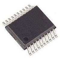
PIC16F1828-I/SS Microchip Technology, PIC16F1828-I/SS Datasheet - Page 257

PIC16F1828-I/SS
Manufacturer Part Number
PIC16F1828-I/SS
Description
IC PIC MCU 8BIT 14KB FLSH 20SSOP
Manufacturer
Microchip Technology
Series
PIC® XLP™ 16Fr
Datasheets
1.PIC16F722-ISS.pdf
(8 pages)
2.PIC16F1826-IP.pdf
(40 pages)
3.PIC16F1824-ISL.pdf
(2 pages)
4.PIC16F1824-ISL.pdf
(419 pages)
5.PIC16F1824-ISL.pdf
(10 pages)
Specifications of PIC16F1828-I/SS
Core Size
8-Bit
Program Memory Size
7KB (4K x 14)
Core Processor
PIC
Speed
32MHz
Connectivity
I²C, SPI, UART/USART
Peripherals
Brown-out Detect/Reset, POR, PWM, WDT
Number Of I /o
17
Program Memory Type
FLASH
Eeprom Size
256 x 8
Ram Size
256 x 8
Voltage - Supply (vcc/vdd)
1.8 V ~ 5.5 V
Data Converters
A/D 12x10b
Oscillator Type
Internal
Operating Temperature
-40°C ~ 85°C
Package / Case
20-SSOP (0.200", 5.30mm Width)
Controller Family/series
PIC16F
No. Of I/o's
18
Eeprom Memory Size
256Byte
Ram Memory Size
256Byte
Cpu Speed
32MHz
No. Of Timers
5
Lead Free Status / RoHS Status
Lead free / RoHS Compliant
Available stocks
Company
Part Number
Manufacturer
Quantity
Price
Part Number:
PIC16F1828-I/SS
Manufacturer:
MIC
Quantity:
20 000
- PIC16F722-ISS PDF datasheet
- PIC16F1826-IP PDF datasheet #2
- PIC16F1824-ISL PDF datasheet #3
- PIC16F1824-ISL PDF datasheet #4
- PIC16F1824-ISL PDF datasheet #5
- Current page: 257 of 419
- Download datasheet (4Mb)
25.4.4 SDA HOLD TIME
The hold time of the SDA pin is selected by the SDAHT
bit of the SSP1CON3 register. Hold time is the time
SDA is held valid after the falling edge of SCL. Setting
the SDAHT bit selects a longer 300 ns minimum hold
time and may help on buses with large capacitance.
TABLE 25-2:
2010 Microchip Technology Inc.
Transmitter
Receiver
Master
Slave
Multi-master
Arbitration
Synchronization Procedure to synchronize the
Idle
Active
Addressed
Slave
Matching
Address
Write Request
Read Request
Clock Stretching When a device on the bus hold
Bus Collision
TERM
I
2
The device which shifts data out
onto the bus.
The device which shifts data in
from the bus.
The device that initiates a transfer,
generates clock signals and termi-
nates a transfer.
The device addressed by the mas-
ter.
A bus with more than one device
that can initiate data transfers.
Procedure to ensure that only one
master at a time controls the bus.
Winning arbitration ensures that
the message is not corrupted.
clocks of two or more devices on
the bus.
No master is controlling the bus,
and both SDA and SCL lines are
high.
Any time one or more master
devices are controlling the bus.
Slave device that has received a
matching address and is actively
being clocked by a master.
Address byte that is clocked into a
slave that matches the value
stored in SSP1ADD.
Slave receives a matching
address with R/W bit clear, and is
ready to clock in data.
Master sends an address byte with
the R/W bit set, indicating that it
wishes to clock data out of the
Slave. This data is the next and all
following bytes until a Restart or
Stop.
SCL low to stall communication.
Any time the SDA line is sampled
low by the module while it is out-
putting and expected high state.
C BUS TERMS
Description
Preliminary
PIC16(L)F1824/1828
DS41419B-page 257
Related parts for PIC16F1828-I/SS
Image
Part Number
Description
Manufacturer
Datasheet
Request
R

Part Number:
Description:
IC, 8BIT MCU, PIC16F, 32MHZ, SOIC-18
Manufacturer:
Microchip Technology
Datasheet:

Part Number:
Description:
IC, 8BIT MCU, PIC16F, 32MHZ, SSOP-20
Manufacturer:
Microchip Technology
Datasheet:

Part Number:
Description:
IC, 8BIT MCU, PIC16F, 32MHZ, DIP-18
Manufacturer:
Microchip Technology
Datasheet:

Part Number:
Description:
IC, 8BIT MCU, PIC16F, 32MHZ, QFN-28
Manufacturer:
Microchip Technology
Datasheet:

Part Number:
Description:
IC, 8BIT MCU, PIC16F, 32MHZ, QFN-28
Manufacturer:
Microchip Technology
Datasheet:

Part Number:
Description:
IC, 8BIT MCU, PIC16F, 32MHZ, QFN-28
Manufacturer:
Microchip Technology
Datasheet:

Part Number:
Description:
IC, 8BIT MCU, PIC16F, 32MHZ, SSOP-20
Manufacturer:
Microchip Technology
Datasheet:

Part Number:
Description:
IC, 8BIT MCU, PIC16F, 20MHZ, DIP-40
Manufacturer:
Microchip Technology
Datasheet:

Part Number:
Description:
IC, 8BIT MCU, PIC16F, 32MHZ, QFN-28
Manufacturer:
Microchip Technology
Datasheet:

Part Number:
Description:
IC, 8BIT MCU, PIC16F, 20MHZ, MQFP-44
Manufacturer:
Microchip Technology
Datasheet:

Part Number:
Description:
IC, 8BIT MCU, PIC16F, 20MHZ, QFN-20
Manufacturer:
Microchip Technology
Datasheet:

Part Number:
Description:
IC, 8BIT MCU, PIC16F, 32MHZ, QFN-28
Manufacturer:
Microchip Technology
Datasheet:

Part Number:
Description:
MCU 14KB FLASH 768B RAM 64-TQFP
Manufacturer:
Microchip Technology
Datasheet:

Part Number:
Description:
7 KB Flash, 384 Bytes RAM, 32 MHz Int. Osc, 16 I/0, Enhanced Mid Range Core, Low
Manufacturer:
Microchip Technology

Part Number:
Description:
14KB Flash, 512B RAM, 256B EEPROM, LCD, 1.8-5.5V 40 UQFN 5x5x0.5mm TUBE
Manufacturer:
Microchip Technology
Datasheet:


