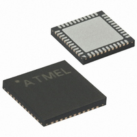
ATMEGA32A-MNR Atmel, ATMEGA32A-MNR Datasheet - Page 167

ATMEGA32A-MNR
Manufacturer Part Number
ATMEGA32A-MNR
Description
IC MCU AVR 32K 16MHZ 44VQFN
Manufacturer
Atmel
Series
AVR® ATmegar
Datasheet
1.ATMEGA32A-MU.pdf
(353 pages)
Specifications of ATMEGA32A-MNR
Core Processor
AVR
Core Size
8-Bit
Speed
16MHz
Connectivity
I²C, SPI, UART/USART
Peripherals
Brown-out Detect/Reset, POR, PWM, WDT
Number Of I /o
32
Program Memory Size
32KB (16K x 16)
Program Memory Type
FLASH
Eeprom Size
1K x 8
Ram Size
2K x 8
Voltage - Supply (vcc/vdd)
2.7 V ~ 5.5 V
Data Converters
A/D 8x10b
Oscillator Type
Internal
Operating Temperature
-40°C ~ 85°C
Package / Case
44-VFQFN Exposed Pad
Lead Free Status / RoHS Status
Lead free / RoHS Compliant
Available stocks
Company
Part Number
Manufacturer
Quantity
Price
- Current page: 167 of 353
- Download datasheet (6Mb)
19.11 Register Description
19.11.1
8155C–AVR–02/11
UDR – USART I/O Data Register
The following code example shows how to read the UCSRC Register contents.
Note:
The assembly code example returns the UCSRC value in r16.
Reading the UBRRH contents is not an atomic operation and therefore it can be read as an ordi-
nary register, as long as the previous instruction did not access the register location.
The USART Transmit Data Buffer Register and USART Receive Data Buffer Registers share the
same I/O address referred to as USART Data Register or UDR. The Transmit Data Buffer Reg-
ister (TXB) will be the destination for data written to the UDR Register location. Reading the
UDR Register location will return the contents of the Receive Data Buffer Register (RXB).
For 5-bit, 6-bit, or 7-bit characters the upper unused bits will be ignored by the Transmitter and
set to zero by the Receiver.
The transmit buffer can only be written when the UDRE Flag in the UCSRA Register is set. Data
written to UDR when the UDRE Flag is not set, will be ignored by the USART Transmitter. When
data is written to the transmit buffer, and the Transmitter is enabled, the Transmitter will load the
data into the transmit Shift Register when the Shift Register is empty. Then the data will be seri-
ally transmitted on the TxD pin.
The receive buffer consists of a two level FIFO. The FIFO will change its state whenever the
receive buffer is accessed. Due to this behavior of the receive buffer, do not use read modify
write instructions (SBI and CBI) on this location. Be careful when using bit test instructions (SBIC
and SBIS), since these also will change the state of the FIFO.
Bit
Read/Write
Initial Value
Assembly Code Example
C Code Example
USART_ReadUCSRC:
unsigned char USART_ReadUCSRC( void )
{
}
; Read UCSRC
in r16,UBRRH
in r16,UCSRC
ret
unsigned char ucsrc;
/* Read UCSRC */
ucsrc = UBRRH;
ucsrc = UCSRC;
return ucsrc;
1. See
R/W
“About Code Examples” on page
7
0
(1)
R/W
6
0
(1)
R/W
5
0
R/W
4
0
RXB[7:0]
TXB[7:0]
6.
R/W
3
0
R/W
2
0
R/W
1
0
ATmega32A
R/W
0
0
UDR (Write)
UDR (Read)
167
Related parts for ATMEGA32A-MNR
Image
Part Number
Description
Manufacturer
Datasheet
Request
R

Part Number:
Description:
Manufacturer:
Atmel Corporation
Datasheet:

Part Number:
Description:
Manufacturer:
ATMEL Corporation
Datasheet:

Part Number:
Description:
IC AVR MCU 32K 16MHZ 5V 44-QFN
Manufacturer:
Atmel
Datasheet:

Part Number:
Description:
IC AVR MCU 32K 16MHZ 5V 40DIP
Manufacturer:
Atmel
Datasheet:

Part Number:
Description:
IC AVR MCU 32K 16MHZ 5V 44TQFP
Manufacturer:
Atmel
Datasheet:

Part Number:
Description:
IC AVR MCU 32K 16MHZ IND 40-DIP
Manufacturer:
Atmel
Datasheet:

Part Number:
Description:
IC AVR MCU 32K 16MHZ IND 44-TQFP
Manufacturer:
Atmel
Datasheet:

Part Number:
Description:
MCU AVR 32KB FLASH 16MHZ 44TQFP
Manufacturer:
Atmel
Datasheet:

Part Number:
Description:
MCU AVR 32KB FLASH 16MHZ 44QFN
Manufacturer:
Atmel
Datasheet:

Part Number:
Description:
MCU AVR 32K FLASH 16MHZ 44-TQFP
Manufacturer:
Atmel
Datasheet:

Part Number:
Description:
IC AVR MCU 32K 16MHZ COM 40-DIP
Manufacturer:
Atmel
Datasheet:

Part Number:
Description:
IC AVR MCU 32K 16MHZ COM 44-QFN
Manufacturer:
Atmel
Datasheet:

Part Number:
Description:
IC AVR MCU 32K 16MHZ COM 44-TQFP
Manufacturer:
Atmel
Datasheet:


