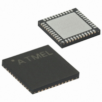
ATMEGA32A-MNR Atmel, ATMEGA32A-MNR Datasheet - Page 281

ATMEGA32A-MNR
Manufacturer Part Number
ATMEGA32A-MNR
Description
IC MCU AVR 32K 16MHZ 44VQFN
Manufacturer
Atmel
Series
AVR® ATmegar
Datasheet
1.ATMEGA32A-MU.pdf
(353 pages)
Specifications of ATMEGA32A-MNR
Core Processor
AVR
Core Size
8-Bit
Speed
16MHz
Connectivity
I²C, SPI, UART/USART
Peripherals
Brown-out Detect/Reset, POR, PWM, WDT
Number Of I /o
32
Program Memory Size
32KB (16K x 16)
Program Memory Type
FLASH
Eeprom Size
1K x 8
Ram Size
2K x 8
Voltage - Supply (vcc/vdd)
2.7 V ~ 5.5 V
Data Converters
A/D 8x10b
Oscillator Type
Internal
Operating Temperature
-40°C ~ 85°C
Package / Case
44-VFQFN Exposed Pad
Lead Free Status / RoHS Status
Lead free / RoHS Compliant
Available stocks
Company
Part Number
Manufacturer
Quantity
Price
- Current page: 281 of 353
- Download datasheet (6Mb)
26.9
26.9.1
8155C–AVR–02/11
SPI Serial Programming Pin Mapping
SPI Serial Programming Algorithm
Table 26-12. Pin Mapping SPI Serial Programming
Figure 26-10. SPI Serial Programming and Verify
Notes:
When programming the EEPROM, an auto-erase cycle is built into the self-timed programming
operation (in the serial mode ONLY) and there is no need to first execute the Chip Erase instruc-
tion. The Chip Erase operation turns the content of every memory location in both the Program
and EEPROM arrays into $FF.
Depending on CKSEL Fuses, a valid clock must be present. The minimum low and high periods
for the serial clock (SCK) input are defined as follows:
Low: > 2 CPU clock cycles for f
High: > 2 CPU clock cycles for f
When writing serial data to the ATmega32A, data is clocked on the rising edge of SCK.
When reading data from the ATmega32A, data is clocked on the falling edge of SCK. See
26-11
To program and verify the ATmega32A in the SPI Serial Programming mode, the following
sequence is recommended (See four byte instruction formats in
for timing details.
1. If the device is clocked by the Internal Oscillator, it is no need to connect a clock source to the
2. V
Symbol
MOSI
MISO
SCK
XTAL1 pin.
CC
-0.3V < AVCC < V
MOSI
MISO
SCK
CC
Pins
ck
ck
PB5
PB6
PB7
< 12MHz, 3 CPU clock cycles for f
< 12MHz, 3 CPU clock cycles for f
+0.3V, however, AVCC should always be within 2.7V - 5.5V
PB5
PB6
PB7
XTAL1
RESET
GND
I/O
O
I
I
(1)
AVCC
VCC
Description
Serial Data in
Serial Data out
Serial Clock
+2.7 - 5.5V
+2.7 - 5.5V
Table
ck
ck
(2)
26-14):
ATmega32A
12MHz
12MHz
Figure
281
Related parts for ATMEGA32A-MNR
Image
Part Number
Description
Manufacturer
Datasheet
Request
R

Part Number:
Description:
Manufacturer:
Atmel Corporation
Datasheet:

Part Number:
Description:
Manufacturer:
ATMEL Corporation
Datasheet:

Part Number:
Description:
IC AVR MCU 32K 16MHZ 5V 44-QFN
Manufacturer:
Atmel
Datasheet:

Part Number:
Description:
IC AVR MCU 32K 16MHZ 5V 40DIP
Manufacturer:
Atmel
Datasheet:

Part Number:
Description:
IC AVR MCU 32K 16MHZ 5V 44TQFP
Manufacturer:
Atmel
Datasheet:

Part Number:
Description:
IC AVR MCU 32K 16MHZ IND 40-DIP
Manufacturer:
Atmel
Datasheet:

Part Number:
Description:
IC AVR MCU 32K 16MHZ IND 44-TQFP
Manufacturer:
Atmel
Datasheet:

Part Number:
Description:
MCU AVR 32KB FLASH 16MHZ 44TQFP
Manufacturer:
Atmel
Datasheet:

Part Number:
Description:
MCU AVR 32KB FLASH 16MHZ 44QFN
Manufacturer:
Atmel
Datasheet:

Part Number:
Description:
MCU AVR 32K FLASH 16MHZ 44-TQFP
Manufacturer:
Atmel
Datasheet:

Part Number:
Description:
IC AVR MCU 32K 16MHZ COM 40-DIP
Manufacturer:
Atmel
Datasheet:

Part Number:
Description:
IC AVR MCU 32K 16MHZ COM 44-QFN
Manufacturer:
Atmel
Datasheet:

Part Number:
Description:
IC AVR MCU 32K 16MHZ COM 44-TQFP
Manufacturer:
Atmel
Datasheet:


