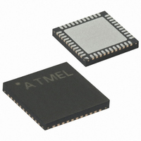
ATMEGA32A-MNR Atmel, ATMEGA32A-MNR Datasheet - Page 64

ATMEGA32A-MNR
Manufacturer Part Number
ATMEGA32A-MNR
Description
IC MCU AVR 32K 16MHZ 44VQFN
Manufacturer
Atmel
Series
AVR® ATmegar
Datasheet
1.ATMEGA32A-MU.pdf
(353 pages)
Specifications of ATMEGA32A-MNR
Core Processor
AVR
Core Size
8-Bit
Speed
16MHz
Connectivity
I²C, SPI, UART/USART
Peripherals
Brown-out Detect/Reset, POR, PWM, WDT
Number Of I /o
32
Program Memory Size
32KB (16K x 16)
Program Memory Type
FLASH
Eeprom Size
1K x 8
Ram Size
2K x 8
Voltage - Supply (vcc/vdd)
2.7 V ~ 5.5 V
Data Converters
A/D 8x10b
Oscillator Type
Internal
Operating Temperature
-40°C ~ 85°C
Package / Case
44-VFQFN Exposed Pad
Lead Free Status / RoHS Status
Lead free / RoHS Compliant
Available stocks
Company
Part Number
Manufacturer
Quantity
Price
- Current page: 64 of 353
- Download datasheet (6Mb)
12.3.4
8155C–AVR–02/11
Alternate Functions of Port D
Table 12-11. Overriding Signals for Alternate Functions in PC3:PC0
Note:
The Port D pins with alternate functions are shown in
Table 12-12. Port D Pins Alternate Functions
The alternate pin configuration is as follows:
• OC2 – Port D, Bit 7
OC2, Timer/Counter2 Output Compare Match output: The PD7 pin can serve as an external out-
put for the Timer/Counter2 Output Compare. The pin has to be configured as an output (DDD7
set (one)) to serve this function. The OC2 pin is also the output pin for the PWM mode timer
function.
• ICP1 – Port D, Bit 6
ICP1 – Input Capture Pin: The PD6 pin can act as an Input Capture pin for Timer/Counter1.
Signal
Name
PUOE
PUOV
DDOE
DDOV
PVOE
PVOV
DIEOE
DIEOV
DI
AIO
Port Pin
PD7
PD6
PD5
PD4
PD3
PD2
PD1
PD0
1. When enabled, the Two-wire Serial Interface enables slew-rate controls on the output pins
PC0 and PC1. This is not shown in the figure. In addition, spike filters are connected between
the AIO outputs shown in the port figure and the digital logic of the TWI module.
PC3/TMS
JTAGEN
1
JTAGEN
0
0
0
JTAGEN
0
–
TMS
Alternate Function
OC2 (Timer/Counter2 Output Compare Match Output)
ICP1 (Timer/Counter1 Input Capture Pin)
OC1A (Timer/Counter1 Output Compare A Match Output)
OC1B (Timer/Counter1 Output Compare B Match Output)
INT1 (External Interrupt 1 Input)
INT0 (External Interrupt 0 Input)
TXD (USART Output Pin)
RXD (USART Input Pin)
PC2/TCK
JTAGEN
1
JTAGEN
0
0
0
JTAGEN
0
–
TCK
PC1/SDA
TWEN
PORTC1 • PUD
TWEN
SDA_OUT
TWEN
0
0
0
–
SDA INPUT
Table
12-12.
(1)
ATmega32A
SCL INPUT
PC0/SCL
TWEN
PORTC0 • PUD
TWEN
SCL_OUT
TWEN
0
0
0
–
64
Related parts for ATMEGA32A-MNR
Image
Part Number
Description
Manufacturer
Datasheet
Request
R

Part Number:
Description:
Manufacturer:
Atmel Corporation
Datasheet:

Part Number:
Description:
Manufacturer:
ATMEL Corporation
Datasheet:

Part Number:
Description:
IC AVR MCU 32K 16MHZ 5V 44-QFN
Manufacturer:
Atmel
Datasheet:

Part Number:
Description:
IC AVR MCU 32K 16MHZ 5V 40DIP
Manufacturer:
Atmel
Datasheet:

Part Number:
Description:
IC AVR MCU 32K 16MHZ 5V 44TQFP
Manufacturer:
Atmel
Datasheet:

Part Number:
Description:
IC AVR MCU 32K 16MHZ IND 40-DIP
Manufacturer:
Atmel
Datasheet:

Part Number:
Description:
IC AVR MCU 32K 16MHZ IND 44-TQFP
Manufacturer:
Atmel
Datasheet:

Part Number:
Description:
MCU AVR 32KB FLASH 16MHZ 44TQFP
Manufacturer:
Atmel
Datasheet:

Part Number:
Description:
MCU AVR 32KB FLASH 16MHZ 44QFN
Manufacturer:
Atmel
Datasheet:

Part Number:
Description:
MCU AVR 32K FLASH 16MHZ 44-TQFP
Manufacturer:
Atmel
Datasheet:

Part Number:
Description:
IC AVR MCU 32K 16MHZ COM 40-DIP
Manufacturer:
Atmel
Datasheet:

Part Number:
Description:
IC AVR MCU 32K 16MHZ COM 44-QFN
Manufacturer:
Atmel
Datasheet:

Part Number:
Description:
IC AVR MCU 32K 16MHZ COM 44-TQFP
Manufacturer:
Atmel
Datasheet:


