ASD5020L640INT Arctic Silicon Devices, ASD5020L640INT Datasheet - Page 2
ASD5020L640INT
Manufacturer Part Number
ASD5020L640INT
Description
ADC (A/D Converters) Mul-Md 12bit/640MSPS 8-bit 1000 MSPS ADC
Manufacturer
Arctic Silicon Devices
Datasheet
1.ASD5020L640INT.pdf
(34 pages)
Specifications of ASD5020L640INT
Number Of Converters
1
Number Of Adc Inputs
2
Conversion Rate
640 MSPs
Resolution
12 bit
Snr
70 dB
Voltage Reference
1 V
Supply Voltage (max)
2 V
Supply Voltage (min)
1.7 V
Maximum Power Dissipation
490 mW
Maximum Operating Temperature
+ 85 C
Mounting Style
SMD/SMT
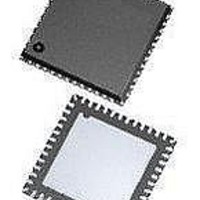
Package / Case
QFN-48
Input Voltage
1.8 V
Minimum Operating Temperature
- 40 C
Lead Free Status / RoHS Status
Lead free / RoHS Compliant


Preliminary Product Specification
Table of Contents
Blizzard Product family: Products and Relations..................................................................................................................3
Specifications........................................................................................................................................................................ 4
Digital and Switching Specifications...................................................................................................................................... 6
Absolute Maximum Ratings.................................................................................................................................................. 7
Pin Configuration and Description......................................................................................................................................... 8
Startup Initialization............................................................................................................................................................. 10
Serial Interface.................................................................................................................................................................... 10
Timing Diagrams................................................................................................................................................................. 11
Register Map....................................................................................................................................................................... 13
Register Description ........................................................................................................................................................... 15
Theory of Operation............................................................................................................................................................ 30
Recommended Usage........................................................................................................................................................ 30
Application Usage Example................................................................................................................................................ 32
Package Mechanical Data.................................................................................................................................................. 33
Product Information............................................................................................................................................................. 34
Ordering information........................................................................................................................................................... 34
Datasheet status................................................................................................................................................................. 34
ASD5020
ASD5020 High Speed Mode........................................................................................................................................... 5
Timing Diagram............................................................................................................................................................. 10
Software Reset.............................................................................................................................................................. 15
Modes of Operation ...................................................................................................................................................... 15
Input Select.................................................................................................................................................................... 16
Full-scale Control .......................................................................................................................................................... 17
Current Control.............................................................................................................................................................. 17
Start-up and Clock Jitter Control................................................................................................................................... 19
LVDS Output Configuration and Control........................................................................................................................21
LVDS Drive Strength Programmability.......................................................................................................................... 24
LVDS Internal Termination Programmability..................................................................................................................24
Power Mode Control ..................................................................................................................................................... 26
Programmable Gain...................................................................................................................................................... 27
Analog Input Invert........................................................................................................................................................ 29
LVDS Test Patterns........................................................................................................................................................ 29
Interleaving Effects and Sampling Order....................................................................................................................... 30
Analog Input.................................................................................................................................................................. 30
Clock Input and Jitter Considerations............................................................................................................................ 31
Start-up Initialization...................................................................................................................................................... 32
Change Mode................................................................................................................................................................ 32
Select Analog Input........................................................................................................................................................ 32
QFN48........................................................................................................................................................................... 33
Objective Product Specification:.................................................................................................................................... 34
Preliminary Product Specification:................................................................................................................................. 34
Product Specification:.................................................................................................................................................... 34
DC-Coupling............................................................................................................................................................ 31
AC-Coupling............................................................................................................................................................. 31
Life Support Applications :....................................................................................................................................... 34
rev 2.0, 2010.11.08
Page 2 of 34
High Speed Mode
Related parts for ASD5020L640INT
Image
Part Number
Description
Manufacturer
Datasheet
Request
R

Part Number:
Description:
ADC (A/D Converters) 13 bit 1 Ch 20 MSPS
Manufacturer:
Arctic Silicon Devices

Part Number:
Description:
ADC (A/D Converters) 12 bit 8 Ch 40 MSPS
Manufacturer:
Arctic Silicon Devices
Part Number:
Description:
ADC (A/D Converters) 13 bit 1 Ch 65 MSPS
Manufacturer:
Arctic Silicon Devices
Part Number:
Description:
ADC (A/D Converters) 10 bit 1 Ch 65 MSPS
Manufacturer:
Arctic Silicon Devices

Part Number:
Description:
ADC (A/D Converters) 10 bit 2 Ch 20 MSPS
Manufacturer:
Arctic Silicon Devices
Part Number:
Description:
ADC (A/D Converters) 13 bit 2 Ch 80 MSPS
Manufacturer:
Arctic Silicon Devices
Part Number:
Description:
ADC (A/D Converters) 12 bit 8 Ch 80 MSPS
Manufacturer:
Arctic Silicon Devices
Part Number:
Description:
ADC (A/D Converters) 10 bit 1 Ch 80 MSPS
Manufacturer:
Arctic Silicon Devices
Part Number:
Description:
ADC (A/D Converters) 10 bit 1 Ch 20 MSPS
Manufacturer:
Arctic Silicon Devices
Part Number:
Description:
ADC (A/D Converters) 13 bit 2 Ch 40 MSPS
Manufacturer:
Arctic Silicon Devices
Part Number:
Description:
ADC (A/D Converters) 10 bit 2 Ch 80 MSPS
Manufacturer:
Arctic Silicon Devices
Part Number:
Description:
ADC (A/D Converters) 10 bit 2 Ch 65 MSPS
Manufacturer:
Arctic Silicon Devices

Part Number:
Description:
ADC (A/D Converters) A-D Conv, Dig Gain Dual 8 bit 500MSPS
Manufacturer:
Arctic Silicon Devices
Datasheet:
Part Number:
Description:
ADC (A/D Converters) A-D Conv, Dig Gain Single 8 bit 1 GSPS
Manufacturer:
Arctic Silicon Devices
Datasheet:
Part Number:
Description:
ADC (A/D Converters) 12 bit 8 Ch 20 MSPS
Manufacturer:
Arctic Silicon Devices