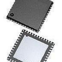
ASD5020L640INT Arctic Silicon Devices, ASD5020L640INT Datasheet - Page 21

ASD5020L640INT
Manufacturer Part Number
ASD5020L640INT
Description
ADC (A/D Converters) Mul-Md 12bit/640MSPS 8-bit 1000 MSPS ADC
Manufacturer
Arctic Silicon Devices
Datasheet
1.ASD5020L640INT.pdf
(34 pages)
Specifications of ASD5020L640INT
Number Of Converters
1
Number Of Adc Inputs
2
Conversion Rate
640 MSPs
Resolution
12 bit
Snr
70 dB
Voltage Reference
1 V
Supply Voltage (max)
2 V
Supply Voltage (min)
1.7 V
Maximum Power Dissipation
490 mW
Maximum Operating Temperature
+ 85 C
Mounting Style
SMD/SMT
Package / Case
QFN-48
Input Voltage
1.8 V
Minimum Operating Temperature
- 40 C
Lead Free Status / RoHS Status
Lead free / RoHS Compliant
Preliminary Product Specification
LVDS Output Configuration and Control
The ASD5020 serial LVDS output has four different modes selected by the register lvds_output_mode as defined in table
14. Power down mode, as described in section 'Startup Initialization', must be activated after or during a change in the
number of output bits to ensure correct behavior.
For the high speed modes only the 12, 14 and 16-bit LVDS output modes are available. When 14 or 16 bit LVDS output
mode is selected the output data will be a 13 bit left justified word filled up with '0's on the LSB side. The different high
speed modes uses the LVDS outputs as defined by table 15.
Maximum data output bit-rate for the ASD5020 is 1 Gb/s. The maximum sampling rate for the different configurations is
given by table 16. The sampling rate is set by the frequency of the input clock (F
the FCLK signal on the LVDS outputs, depends on the selected mode and the sampling frequency (F
table 17.
ASD5020
lvds_output_mode
<2:0>
low_clk_freq
lvds_advance
lvds_delay
phase_ddr<1:0>
btc_mode
msb_first
Name
lvds_output_mode<2:0>
Sets the number of LVDS output bits.
Low clock frequency used.
Advance LVDS data bits and frame
clock by one clock cycle
Delay LVDS data bits and frame clock
by one clock cycle
Controls the phase of the LCLK
output relative to data.
Binary two's complement format for
ADC output data.
Serialized ADC output data comes out
with MSB first.
Single channel
Dual channel, channel 1
Dual channel, channel 2
Quad channel, channel 1
Quad channel, channel 2
Quad channel, channel 3
Quad channel, channel 4
High speed modes/ channels
Other
000
001
010
011
Description
Table 15: High speed modes and use of LVDS outputs
Table 14: Number of bits in LVDS output
Number of bits
Do not use
12 bit
14 bit
16 bit
8 bit
Straight offset binary
D1A, D1B, D2A, D2B, D3A, D3B, D4A, D4B
D1A, D1B, D2A, D2B
D3A, D3B, D4A, D4B
D1A, D1B
D2A, D2B
D3A, D3B
D4A, D4B
rev 2.0, 2010.11.08
90 degrees
Default
LSB first
Inactive
Inactive
Inactive
Page 21 of 34
12 bit
D15 D14D13D12D11D10 D9 D8 D7 D6 D5 D4 D3 D2 D1 D0
Default setting for High Speed Modes
8 bit mode, up to 1GSPS (ASD5010)
LVDS outputs used
Comment
S
). The frame-rate, i.e. the frequency of
X X
X 0
0 X
X
X
High Speed Mode
X X X
X
S
) as defined in
Address
0x53
0x42
0x46
Hex


