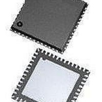
ASD5020L640INT Arctic Silicon Devices, ASD5020L640INT Datasheet - Page 23

ASD5020L640INT
Manufacturer Part Number
ASD5020L640INT
Description
ADC (A/D Converters) Mul-Md 12bit/640MSPS 8-bit 1000 MSPS ADC
Manufacturer
Arctic Silicon Devices
Datasheet
1.ASD5020L640INT.pdf
(34 pages)
Specifications of ASD5020L640INT
Number Of Converters
1
Number Of Adc Inputs
2
Conversion Rate
640 MSPs
Resolution
12 bit
Snr
70 dB
Voltage Reference
1 V
Supply Voltage (max)
2 V
Supply Voltage (min)
1.7 V
Maximum Power Dissipation
490 mW
Maximum Operating Temperature
+ 85 C
Mounting Style
SMD/SMT
Package / Case
QFN-48
Input Voltage
1.8 V
Minimum Operating Temperature
- 40 C
Lead Free Status / RoHS Status
Lead free / RoHS Compliant
Preliminary Product Specification
To ease timing in the receiver when using multiple ASD5020, the device has the option to adjust the timing of the output
data and the frame clock. The propagation delay with respect to the ADC input clock can be moved one LVDS clock
cycle forward or backward, by using lvds_delay and lvds_advance, respectively. See figure 10 for details. Note that LCLK
is not affected by lvds_delay or lvds_advance settings.
The LVDS output interface of ASD5020 is a DDR interface. The default setting is with the LCLK rising and falling edge
transitions in the middle of alternate data windows. The phase for LCLK can be programmed relative to the output frame
clock and data bits using phase_ddr<1:0>. The LCLK phase modes are shown in figure 11. The default timing is identical
to setting phase_ddr<1:0>='10'.
The default data output format is offset binary. Two's complement mode can be selected by setting the btc_mode bit to '1'
which inverts the MSB.
The first bit of the frame (following the rising edge of FCLKP) is the LSB of the ADC output for default settings.
Programming the msb_first mode results in reverse bit order, and the MSB is output as the first bit following the FCLKP
rising edge.
ASD5020
default:
lvds_delay = '1':
lvds_advance = '1':
PHASE_DDR<1:0>='00' (270 deg)
Dxx<1:0>
Dxx<1:0>
PHASE_DDR<1:0>='10' (90 deg)
Input clock
FCLK
FCLK
LCLK
FCLK
FCLK
LCLK
LCLK
LCLK
FCLK
FCLK
FCLK
LCLK
FCLK
FCLK
FCLK
LCLK
N
Figure 11: Phase programmability modes for LCLK
N
P
P
N
N
P
P
Dxxx
Dxxx
Dxxx
N
N
P
P
N
P
N
P
Figure 10: LVDS output timing adjustment
D3
N-2 N-2 N-2 N-2 N-2 N-2 N-2 N-2 N-2
D2
N-2 N-2 N-2 N-2 N-2 N-2 N-2 N-2 N-2 N-2
D4
N-2 N-2 N-2 N-2 N-2 N-2 N-2 N-2
D4
D3
D5
D5
D4
D6
rev 2.0, 2010.11.08
T
Page 23 of 34
LVDS
D7
D6
D5
T
D7
D8
D6
T
T
PROP
PROP
PROP
D8
D9
D7
PHASE_DDR<1:0>='01' (180 deg)
Dxx<1:0>
Dxx<1:0>
FCLK
FCLK
FCLK
FCLK
LCLK
LCLK
LCLK
LCLK
PHASE_DDR<1:0>='11' (0 deg)
D9
D10 D11 D0
D8
D10 D11 D0
D9
N
P
P
N
P
N
N
P
D10 D11
T
N
LVDS
D1
N
N
D1
D2
T
N
N
D0
N
LVDS
D2
D3
N
N
D1
N
D3
D4
N
N
D2
N
D4
D5
N
N
D3
N
D5
D6
N
N
D4
N
D6
D7
N
N
D5
N
D8
D7
D6
N
N
N
High Speed Mode
D8
D9
N
D7
N
N
D9
D10
N
D8
N
N


