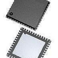
ASD5020L640INT Arctic Silicon Devices, ASD5020L640INT Datasheet - Page 6

ASD5020L640INT
Manufacturer Part Number
ASD5020L640INT
Description
ADC (A/D Converters) Mul-Md 12bit/640MSPS 8-bit 1000 MSPS ADC
Manufacturer
Arctic Silicon Devices
Datasheet
1.ASD5020L640INT.pdf
(34 pages)
Specifications of ASD5020L640INT
Number Of Converters
1
Number Of Adc Inputs
2
Conversion Rate
640 MSPs
Resolution
12 bit
Snr
70 dB
Voltage Reference
1 V
Supply Voltage (max)
2 V
Supply Voltage (min)
1.7 V
Maximum Power Dissipation
490 mW
Maximum Operating Temperature
+ 85 C
Mounting Style
SMD/SMT
Package / Case
QFN-48
Input Voltage
1.8 V
Minimum Operating Temperature
- 40 C
Lead Free Status / RoHS Status
Lead free / RoHS Compliant
Preliminary Product Specification
Digital and Switching Specifications
AVDD= DVDD=OVDD=1.8V, RSDS output data levels, unless otherwise noted
ASD5020
Clock Inputs
DC
Compliance
V
V
V
V
C
Logic inputs (CMOS)
V
V
V
V
I
I
C
Data outputs
Compliance
V
V
V
Output coding
Timing
Characteristics
t
t
t
T
T
T
T
T
T
T
LVDS Output Timing
Characteristics
t
T
T
T
HI
LI
A
j
j
data
skew
SU
SLPCH
OVR
LATHSMQ
LATHSMD
LATHSMS
PROP
EDGE
CLKEDGE
CK,diff
CK,sine
CK,CMOS
CM,CK
CK
HI
HI
LI
LI
I
OUT
OUT
CM
Parameter
Duty Cycle
Differential input voltage swing
Differential input voltage swing, sine wave clock input
Voltage input range CMOS (CLKN connected to ground)
Input common mode voltage. Keep voltages within ground and
voltage of OVDD
Differential Input capacitance
High Level Input Voltage. V
High Level Input Voltage. V
Low Level Input Voltage. V
Low Level Input Voltage. V
High Level Input leakage Current
Low Level Input leakage Current
Input Capacitance
Differential output voltage, LVDS
Differential output voltage, RSDS
Output common mode voltage
Default/optional
Aperture delay
Aperture jitter, all bits set to '1' in jitter_ctrl<7:0>
Aperture jitter, one bit set to '1' in jitter_ctrl<7:0>
Timing skew between ADC channels
Start up time from Power Down Mode and Deep Sleep Mode to
Active Mode in µs. See section "Clock Frequency" for details.
Start up time from Sleep Channel Mode to Active Mode
Out of range recovery time
Pipeline delay, Quad High Speed Mode
Pipeline delay, Dual High Speed Mode
Pipeline delay, Single High Speed Mode
LCLK to data delay time (excluding programmable phase shift)
Clock propagation delay.
LVDS bit-clock duty-cycle
Frame clock cycle-to-cycle jitter
Data rise- and fall time 20% to 80%
Clock rise- and fall time 20% to 80%
OVDD
OVDD
OVDD
OVDD
Description
≥ 3.0V
= 1.7V – 3.0V
≥ 3.0V
= 1.7V – 3.0V
rev 2.0, 2010.11.08
Page 6 of 34
0.8 ·V
6*T
+/-200
+/-800
Offset Binary/ 2's complement
+2.2
Min
0.3
40
45
2
0
0
LVDS
CMOS, LVDS, LVPECL
OVDD
LVDS / RSDS
7*T
V
+3.5
Typ
350
150
120
160
128
OVDD
1.2
1.5
2.5
0.5
0.7
0.7
15
50
32
64
3
3
1
LVDS
V
0.2 ·V
High Speed Mode
7*T
OVDD
+/-10
+/-10
Max
+5.0
0.8
2.5
60
55
LVDS
OVDD
-0.3 V
% high
mVpp
mVpp
pF
V
V
V
V
µA
µA
pF
mV
mV
V
ns
fsrms
fsrms
psrms
µs
µs
clock
cycles
clock
cycles
clock
cycles
clock
cycles
ps
ns
% LCLK
cycle
% LCLK
cycle
Unit
ns
ns


