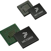
MC13892AJVL Freescale Semiconductor, MC13892AJVL Datasheet - Page 104

MC13892AJVL
Manufacturer Part Number
MC13892AJVL
Description
IC PMU I.MX51/37/35/27 186MAPBGA
Manufacturer
Freescale Semiconductor
Datasheets
1.MC13892AJVLR2.pdf
(156 pages)
2.MC13892AJVLR2.pdf
(2 pages)
3.MC13892AJVLR2.pdf
(16 pages)
4.MC13892AJVLR2.pdf
(5 pages)
Specifications of MC13892AJVL
Applications
Battery Management, Display (LED Drivers), Handheld/Mobile Devices, Power Supply
Operating Temperature
-40°C ~ 85°C
Mounting Type
Surface Mount
Package / Case
186-LFBGA
Mounting Style
SMD/SMT
Duty Cycle (max)
55 %
Input Voltage
- 0.3 V to + 20 V
Maximum Operating Temperature
+ 85 C
Minimum Operating Temperature
- 30 C
Output Current
30 mA
Output Voltage
3.3 V
Topology
Boost
Operating Temperature (max)
85C
Operating Temperature (min)
-40C
Mounting
Surface Mount
Package Type
BGA
Case Length
12mm
Screening Level
Industrial
Lead Free Status / RoHS Status
Lead free / RoHS Compliant
Current - Supply
-
Voltage - Supply
-
Lead Free Status / Rohs Status
Lead free / RoHS Compliant
Available stocks
Company
Part Number
Manufacturer
Quantity
Price
Company:
Part Number:
MC13892AJVL
Manufacturer:
Freescale Semiconductor
Quantity:
10 000
Part Number:
MC13892AJVL
Manufacturer:
FREESCALE
Quantity:
20 000
Company:
Part Number:
MC13892AJVLR2
Manufacturer:
Freescale Semiconductor
Quantity:
10 000
FUNCTIONAL DEVICE OPERATION
ADC SUBSYSTEM
ADC ARBITRATION
store both their results as shown in
access to the control of 'ADC BIS' is handled via the ADCBISn bits located at bit position 23 of the ADC control registers, which
functions as an extended address bit. By setting this bit to a 1, the control bits which follow are destined for the 'ADC BIS'.
ADCBISn will always read back 0 and there is no read access to the control bits related to 'ADC BIS'. The read results from the
'ADC' and 'ADC BIS' conversions are available in two separate registers.
104
13892
The ADC converter and its control is based on a single ADC converter core with the possibility to store two requests, and to
The programming for the two requests, the one to the 'ADC' and to the 'ADC BIS', uses the same SPI registers. The write
The following diagram schematically shows how the ADC control and result registers are set-up.
Table 93. Die Temperature Voltage Reading
Table 94. ADC Channel 7 Scaling Selection
Die Temperature Read Out Code at 25 °C
Temperature change per LSB
Slope error
ADIN7DIV
0
1
0
1
x
x
ADIN7SEL1
Parameter
0
0
0
1
1
1
Figure
27. This allows two independent pieces of software to perform ADC requests.
Figure 27. ADC Request Handling
ADIN7SEL0
0
0
1
0
1
1
Minimum
General purpose input ADIN7, Scaling = 1
General purpose input ADIN7, Scaling = 1 / 2
Die temperature
UID pin voltage, Scaling = 1 / 2
General purpose input ADIN7B, Scaling = 1
General purpose input ADIN7B, Scaling = 1 / 2
-
-
-
Channel 7 Routing and Scaling
+0.4244 °C
Typical
680
-
Analog Integrated Circuit Device Data
Maximum
5.0
-
-
Freescale Semiconductor
Decimal
°C/LSB
Unit
%


