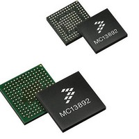
MC13892AJVL Freescale Semiconductor, MC13892AJVL Datasheet - Page 37

MC13892AJVL
Manufacturer Part Number
MC13892AJVL
Description
IC PMU I.MX51/37/35/27 186MAPBGA
Manufacturer
Freescale Semiconductor
Datasheets
1.MC13892AJVLR2.pdf
(156 pages)
2.MC13892AJVLR2.pdf
(2 pages)
3.MC13892AJVLR2.pdf
(16 pages)
4.MC13892AJVLR2.pdf
(5 pages)
Specifications of MC13892AJVL
Applications
Battery Management, Display (LED Drivers), Handheld/Mobile Devices, Power Supply
Operating Temperature
-40°C ~ 85°C
Mounting Type
Surface Mount
Package / Case
186-LFBGA
Mounting Style
SMD/SMT
Duty Cycle (max)
55 %
Input Voltage
- 0.3 V to + 20 V
Maximum Operating Temperature
+ 85 C
Minimum Operating Temperature
- 30 C
Output Current
30 mA
Output Voltage
3.3 V
Topology
Boost
Operating Temperature (max)
85C
Operating Temperature (min)
-40C
Mounting
Surface Mount
Package Type
BGA
Case Length
12mm
Screening Level
Industrial
Lead Free Status / RoHS Status
Lead free / RoHS Compliant
Current - Supply
-
Voltage - Supply
-
Lead Free Status / Rohs Status
Lead free / RoHS Compliant
Available stocks
Company
Part Number
Manufacturer
Quantity
Price
Company:
Part Number:
MC13892AJVL
Manufacturer:
Freescale Semiconductor
Quantity:
10 000
Part Number:
MC13892AJVL
Manufacturer:
FREESCALE
Quantity:
20 000
Company:
Part Number:
MC13892AJVLR2
Manufacturer:
Freescale Semiconductor
Quantity:
10 000
CONTROL LOGIC
LICELL
If the main battery is deeply discharged, removed, or contact-bounced (i.e., during a power cut), the RTC system and coin cell
maintained logic will switch over to the LICELL for backup power. This pin also works as a current-limited voltage source for
battery charging. A small capacitor should be placed from LICELL to ground under all circumstances.
XTAL1
XTAL2
GNDRTC
CLK32K
reference), which is referenced to SPIVCC. The CLK32K is restricted to state machine activation in normal on mode.
CLK32KMCU
to the system processor) referenced to VSRTC. The driver is enabled by the start-up sequencer and the CLK32KMCU is
programmable for Low Power Off mode control by the state machine.
RESETB AND RESETBMCU
Functional Device Operation on page
to keep one in reset while the other is up and running.
WDI
connected to SW4 = 1.8 V). SPIVCC must therefore remain enabled to allow for proper WDI detection. If WDI goes low, the
system will transition to the Off state or Cold Start (depending on the configuration).
STANDBY AND STANDBYSEC
the application processor (which typically controls the STANDBY pin) and peripherals (which typically control the STANDBYSEC
pin) allow it. This is referred to as a Standby event.
account the programmed input polarities associated with each pin. Since the Standby pin activity is driven asynchronously to the
system, a finite time is required for the internal logic to qualify and respond to the pin level changes.
Watchdog phase. This allows the system to power up without concern of the required Standby polarities, since software can
make adjustments accordingly, as soon as it is running.
INT
Analog Integrated Circuit Device Data
Freescale Semiconductor
Coin cell supply input and charger output. The LICELL pin provides a connection for a coin cell backup battery or supercap.
32.768 kHz Oscillator crystal connection 1.
32.768 kHz Oscillator crystal connection 2.
Ground for the RTC block.
32 kHz Clock output for peripherals. At system start-up, the 32 kHz clock is driven to CLK32K (provided as a peripheral clock
32 kHz Clock output for processor. At system start-up, the 32 kHz clock is driven to CLK32KMCU (intended as the CKIL input
Reset output for peripherals and processor respectively. These depend on the Power Control Modes of operation
Watchdog input. This pin must be high to stay in the On mode. The WDI IO supply voltage is referenced to SPIVCC (normally
Standby input signal from processor and from peripherals respectively.
To ensure that shared resources are properly powered when required, the system will only be allowed into Standby when both
The Standby pins are programmable for Active High or Active Low polarity, and that decoding of a Standby event will take into
The state of the Standby pins only have influence in the On mode and are therefore ignored during start up and in the
Interrupt to processor. Unmasked interrupt events are signaled to the processor by driving the INT pin high.
41). These are meant as reset for the processor, or peripherals in a power up condition, or
FUNCTIONAL PIN DESCRIPTION
FUNCTIONAL DESCRIPTION
(See
13892
37


