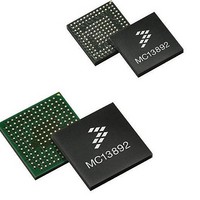
MC13892JVL Freescale Semiconductor, MC13892JVL Datasheet - Page 10

MC13892JVL
Manufacturer Part Number
MC13892JVL
Description
IC PMU I.MX51/37/35/27 186MAPBGA
Manufacturer
Freescale Semiconductor
Datasheets
1.MC13892AJVLR2.pdf
(156 pages)
2.MC13892AJVLR2.pdf
(2 pages)
3.MC13892AJVLR2.pdf
(16 pages)
4.MC13892JVL.pdf
(161 pages)
Specifications of MC13892JVL
Applications
Battery Management, Display (LED Drivers), Handheld/Mobile Devices, Power Supply
Operating Temperature
-40°C ~ 85°C
Mounting Type
Surface Mount
Package / Case
186-LFBGA
Output Current
65 mA
Output Voltage
1.5 V
Operating Temperature (max)
85C
Operating Temperature (min)
-40C
Mounting
Surface Mount
Package Type
BGA
Case Length
12mm
Screening Level
Industrial
Lead Free Status / RoHS Status
Lead free / RoHS Compliant
Current - Supply
-
Voltage - Supply
-
Lead Free Status / Rohs Status
Lead free / RoHS Compliant
Available stocks
Company
Part Number
Manufacturer
Quantity
Price
Company:
Part Number:
MC13892JVL
Manufacturer:
DALSA
Quantity:
4
Company:
Part Number:
MC13892JVL
Manufacturer:
Freescale Semiconductor
Quantity:
10 000
Part Number:
MC13892JVL
Manufacturer:
FREESCALE
Quantity:
20 000
Company:
Part Number:
MC13892JVLR2
Manufacturer:
Freescale Semiconductor
Quantity:
10 000
6
6.1
To place and route adequately external switcher components, follow the current paths of a Buck converter, as shown
in
There are paths of 2 colors and paths with only one-color. Special attention must be paid to the one-color paths,
because there the current alternates between zero and full value. These one-color paths are areas with high di/dt,
that generate a significant magnetic field around the PCB traces.
It is important that all of these critical traces must be kept as short as possible. Each trace has an inductance
proportional to the length. Inductance cannot tolerate high di/dt, so a high di/dt in long traces will result in a high
ringing dv/dt. A wide trace is not a compensating solution for a long trace, as inductance is NOT inversely
proportional to the width of the trace.
Traces must be very short and fairly wide (large amount of current flow in these traces), and should not go through
any vias, as they also add impedance and inductance. Switcher components such as inductors and capacitors
should be as close to the IC as possible to achieve a proper trace length.
Make sure that each trace is capable of handling the current it will carry. As a rule of thumb, it can be considered
that a 10 mil trace with a thickness of 1.0 oz/ft
1.3 A in a 1.0 oz/ft
must be 13 mils wide.
10
13892
SWITCHING POWER SUPPLIES TRACES
Figure 9
Switching Power Supplies Traces
Buck Converter
and
Figure
2
copper layer (as could be the case with an SW1 signal, because of the transient off the caps),
10.
Figure 10. Critical traces of a buck converter.
Figure 9. Current flow on a buck converter.
2
, is capable of handling 1.0 ampere. Therefore, a trace that will carry
FB
FB
VIN
VIN
LX
LX
If a schottcky diode is
anticipated
High di/dt trace
High di/dt traces if
schottky diode added
ON phase
OFF phase
Analog Integrated Circuit Device Data
Freescale Semiconductor


