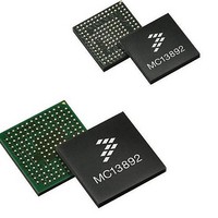
MC13892JVL Freescale Semiconductor, MC13892JVL Datasheet - Page 13

MC13892JVL
Manufacturer Part Number
MC13892JVL
Description
IC PMU I.MX51/37/35/27 186MAPBGA
Manufacturer
Freescale Semiconductor
Datasheets
1.MC13892AJVLR2.pdf
(156 pages)
2.MC13892AJVLR2.pdf
(2 pages)
3.MC13892AJVLR2.pdf
(16 pages)
4.MC13892JVL.pdf
(161 pages)
Specifications of MC13892JVL
Applications
Battery Management, Display (LED Drivers), Handheld/Mobile Devices, Power Supply
Operating Temperature
-40°C ~ 85°C
Mounting Type
Surface Mount
Package / Case
186-LFBGA
Output Current
65 mA
Output Voltage
1.5 V
Operating Temperature (max)
85C
Operating Temperature (min)
-40C
Mounting
Surface Mount
Package Type
BGA
Case Length
12mm
Screening Level
Industrial
Lead Free Status / RoHS Status
Lead free / RoHS Compliant
Current - Supply
-
Voltage - Supply
-
Lead Free Status / Rohs Status
Lead free / RoHS Compliant
Available stocks
Company
Part Number
Manufacturer
Quantity
Price
Company:
Part Number:
MC13892JVL
Manufacturer:
DALSA
Quantity:
4
Company:
Part Number:
MC13892JVL
Manufacturer:
Freescale Semiconductor
Quantity:
10 000
Part Number:
MC13892JVL
Manufacturer:
FREESCALE
Quantity:
20 000
Company:
Part Number:
MC13892JVLR2
Manufacturer:
Freescale Semiconductor
Quantity:
10 000
7
To compensate for the voltage drop on the MC13892 power management IC switchers line due to the PCB wire
resistance, the PCB wire resistance needs to be placed inside the closed loop of the switcher. The goal is to stabilize
the voltage on that switcher line output.
The capacitor and coil components L and C are usually placed close to the MC13892 package. The voltage,
SWxOUT, is equal to the programmed output switcher voltage, minus the dropout caused by the PCB trace. This
dropout is also dependent on the DC load current on SWxOUT. In a typical configuration, the feedback loop is not
usually shielded.
The feedback signal is the core of the loop, with the functional information fed back and compared for reference (this
trace must be shielded from other signals). Moreover, it is a very high-impedance signal, so keep its trace thin and
far from the switching signal (the length of this trace does not matter).
Freescale recommends following the L and C configuration as designated. The output capacitor should be placed
near the point where the current is drawn on the output side of the PCB wire resistance, as shown in
PCB wire resistance is now inside the closed loop of the switcher, so it does not impact the DC voltage at SWxOUT.
The switcher feedback trace must be shielded, as this line is attached to a high-impedance point in the MC13892.
Any perturbation on this line must be minimized to ensure the stability of the switcher.
Figure 17
on the switcher line.
Analog Integrated Circuit Device Data
Freescale Semiconductor
Feedback Signals
shows the recommended configuration for the MC13892 power management IC, to stabilize the voltage
Figure 16. Placement and Layout Philosophy for a Recommended PCB.
Figure 15. Critical Traces on a Boost Converter.
Keep VERY short and wide
Keep short and wide
FB
FB
High di/dt trace
High di/dt trace
Low di/dt trace
Lower plane level,
keep far away from
switching signal
FEEDBACK SIGNALS
Figure
14. The
13892
13


