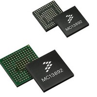
MC13892JVL Freescale Semiconductor, MC13892JVL Datasheet - Page 9

MC13892JVL
Manufacturer Part Number
MC13892JVL
Description
IC PMU I.MX51/37/35/27 186MAPBGA
Manufacturer
Freescale Semiconductor
Datasheets
1.MC13892AJVLR2.pdf
(156 pages)
2.MC13892AJVLR2.pdf
(2 pages)
3.MC13892AJVLR2.pdf
(16 pages)
4.MC13892JVL.pdf
(161 pages)
Specifications of MC13892JVL
Applications
Battery Management, Display (LED Drivers), Handheld/Mobile Devices, Power Supply
Operating Temperature
-40°C ~ 85°C
Mounting Type
Surface Mount
Package / Case
186-LFBGA
Output Current
65 mA
Output Voltage
1.5 V
Operating Temperature (max)
85C
Operating Temperature (min)
-40C
Mounting
Surface Mount
Package Type
BGA
Case Length
12mm
Screening Level
Industrial
Lead Free Status / RoHS Status
Lead free / RoHS Compliant
Current - Supply
-
Voltage - Supply
-
Lead Free Status / Rohs Status
Lead free / RoHS Compliant
Available stocks
Company
Part Number
Manufacturer
Quantity
Price
Company:
Part Number:
MC13892JVL
Manufacturer:
DALSA
Quantity:
4
Company:
Part Number:
MC13892JVL
Manufacturer:
Freescale Semiconductor
Quantity:
10 000
Part Number:
MC13892JVL
Manufacturer:
FREESCALE
Quantity:
20 000
Company:
Part Number:
MC13892JVLR2
Manufacturer:
Freescale Semiconductor
Quantity:
10 000
board from top to bottom, the drill can not be too narrow. The MC13892VK’s small pins do not allow their use, but
MC13892VL does.
Vias placed on the pads of the footprint can have a 12 mil diameter hole, with an 8.0 mil drill for the manufacturer to
be able to use a conductive fill in them. 12 mil diameter vias will allow 9.0 mil traces to pass through them on the
inner and bottom layers of the board, while 16 mil pads of the footprint will only allow 5.0 mil traces on the top layer
below the IC. It is recommended to place high current traces on the bottom layer.
5.0 mil traces passing through 16 mil pads will result in a 5.0 mil separation between the pad and the trace, which
can be made with a 1.0 oz. copper thickness.
Taking advantage of the trough vias, the fanout can be primarily made on the top and bottom layers, for the inner
ones to be completely ground and power.
5
CLK is the fastest signal of the system, so it must be given special care. Here are some tips for routing the
communication signals:
To avoid contamination of these delicate signals by nearby high power or high frequency signals, it is a good practice
to shield them with ground planes placed on adjacent layers. Make sure the ground plane is uniform throughout the
whole signal trace length.
These signals can be placed on an outer layer of the board to reduce their capacitance in respect to the ground
plane.
The crystal connected to pins XTAL1 and XTAL2 must not have a ground plane directly below.
The following are clock signals: CLK, CLK32K, CLK32KMCU, XTAL1, and XTAL2. These signals must not run
parallel to each other, or in the same routing layer. If it is necessary to run clock signals parallel to each other, or
parallel to any other signal, then follow a MAX PARALLEL rule as follows:
Care must be taken with these signals not to contaminate analog signals, as they are high frequency signals.
Another good practice is to trace them perpendicularly on different layers so there is a minimum area of proximity
between signals.
Analog Integrated Circuit Device Data
Freescale Semiconductor
•
•
•
•
SPI/I2C Communication and Real Time Clock Signals
Up to 1 inch parallel length – 25 mil minimum separation.
Up to 2 inch parallel length – 50 mil minimum separation.
Up to 3 inch parallel length – 100 mil minimum separation.
Up to 4 inch parallel length – 250 mil minimum separation.
Figure 8. Recommended Shielding for Critical Signals.
DO
Signal
Ground Plane
SPI/I2C COMMUNICATION AND REAL TIME CLOCK SIGNALS
DON’T!
Signal
Ground Planes
13892
9


