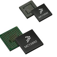
MC13892JVL Freescale Semiconductor, MC13892JVL Datasheet - Page 7

MC13892JVL
Manufacturer Part Number
MC13892JVL
Description
IC PMU I.MX51/37/35/27 186MAPBGA
Manufacturer
Freescale Semiconductor
Datasheets
1.MC13892AJVLR2.pdf
(156 pages)
2.MC13892AJVLR2.pdf
(2 pages)
3.MC13892AJVLR2.pdf
(16 pages)
4.MC13892JVL.pdf
(161 pages)
Specifications of MC13892JVL
Applications
Battery Management, Display (LED Drivers), Handheld/Mobile Devices, Power Supply
Operating Temperature
-40°C ~ 85°C
Mounting Type
Surface Mount
Package / Case
186-LFBGA
Output Current
65 mA
Output Voltage
1.5 V
Operating Temperature (max)
85C
Operating Temperature (min)
-40C
Mounting
Surface Mount
Package Type
BGA
Case Length
12mm
Screening Level
Industrial
Lead Free Status / RoHS Status
Lead free / RoHS Compliant
Current - Supply
-
Voltage - Supply
-
Lead Free Status / Rohs Status
Lead free / RoHS Compliant
Available stocks
Company
Part Number
Manufacturer
Quantity
Price
Company:
Part Number:
MC13892JVL
Manufacturer:
DALSA
Quantity:
4
Company:
Part Number:
MC13892JVL
Manufacturer:
Freescale Semiconductor
Quantity:
10 000
Part Number:
MC13892JVL
Manufacturer:
FREESCALE
Quantity:
20 000
Company:
Part Number:
MC13892JVLR2
Manufacturer:
Freescale Semiconductor
Quantity:
10 000
3.2
4
Pin Escape is defined as the manner by which the signals leaving the IC from their associated pin, can be delivered
on a circuit board trace of a specified size, to a point at which the traces can acquire the size necessary to perform
their process function.
4.1
The most convenient way to approach pin escape is to take the signals coming from the bottom of the IC, with 3.0 mil
traces on the top layer. Micro vias can be put on the pads of the footprint for the signals on the center of the IC.
These will take the signals from the outer layer to the following one, once there, since this layer will not be as
crowded as the top one, 5.0 mil traces can take the signal between the vias. These traces can become bigger once
they are out from the bottom of the IC. More micro vias can be put among the pins to take the signal to another layer.
The recommendation is for the micro vias to have a 10 mil diameter (same as the pads of the footprint) with a 5.0 mil
drill, which along with the 3.0 mil traces, will result in a 3.0 mil separation between the pad and the trace. This can
be done with a 0.5 oz copper thickness on the top layer. The rest of the layers can have 1.0 oz copper thickness for
better current handling. Care must be taken on these layers that the separation is more than 5.0 mils between
traces, vias, pads, and planes. Reference
Analog Integrated Circuit Device Data
Freescale Semiconductor
•
•
•
•
•
•
•
•
•
•
•
•
Place these components first so they are as close as possible to the IC:
Shield feedback paths of the switchers (trace them on the bottom so the ground and power planes shield these traces).
Sense pins must be directly connected to the pads of the sense resistors via separate traces (BATT, BATTISNS,
BATTISNSCC, BPSNS, and CHRGISNS).
BATTISNSCC must be connected directly to the pads of the sense resistor via a separate trace from BATTISNS.
External pass devices of regulators must be closer to the load, but be careful with the sense and drive traces.
Output caps of LDOs with the external pass device option should be close to the transistor (VVIDEO, VCAM, VSD,
VGEN1, VGEN2 and VGEN3).
Avoid a coupling trace between important signal/low noise supplies (like REFCORE) from any switching node.
Ensure each of the components is referenced, or at least it does not have a long return path to the ground of the block
to which it belongs.
Trace REFCORE away from, or shielded from SWLEDOUT
Traces that go from BP to a pin of the MC13892 must reach a capacitor before the pin.
Routes for GNDSW should be suitably large. They will carry heavy switching currents.
Switcher inductors should also be placed close to the IC, and switching node traces should be short and wide, to reduce
conduction losses.
Pin Escape
Component Placement Hints
The MC13892VK Package
– Place input caps of the switchers first (SW1, SW2, SW3, and SW4)
– Place the output diode of the boost (SWBST)
– Place output caps and diodes of the boost (SWBST) and SWLED
– Place the REFCORE cap
Note: A more detailed layer design may be required to route the i.MX. If the
MC13892 is being interfaced with an i.MX, just four of the layers will be needed to
route it. Please note, for the MC13892VK, the fan-out needs to be made on the
layer right next to the top, since micro vias will be needed to take the signals out of
the IC as explained in the Pin Escape section.
Figure
7.
NOTE
PIN ESCAPE
13892
7


