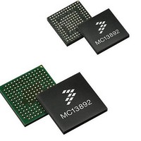
MC13892JVL Freescale Semiconductor, MC13892JVL Datasheet - Page 11

MC13892JVL
Manufacturer Part Number
MC13892JVL
Description
IC PMU I.MX51/37/35/27 186MAPBGA
Manufacturer
Freescale Semiconductor
Datasheets
1.MC13892AJVLR2.pdf
(156 pages)
2.MC13892AJVLR2.pdf
(2 pages)
3.MC13892AJVLR2.pdf
(16 pages)
4.MC13892JVL.pdf
(161 pages)
Specifications of MC13892JVL
Applications
Battery Management, Display (LED Drivers), Handheld/Mobile Devices, Power Supply
Operating Temperature
-40°C ~ 85°C
Mounting Type
Surface Mount
Package / Case
186-LFBGA
Output Current
65 mA
Output Voltage
1.5 V
Operating Temperature (max)
85C
Operating Temperature (min)
-40C
Mounting
Surface Mount
Package Type
BGA
Case Length
12mm
Screening Level
Industrial
Lead Free Status / RoHS Status
Lead free / RoHS Compliant
Current - Supply
-
Voltage - Supply
-
Lead Free Status / Rohs Status
Lead free / RoHS Compliant
Available stocks
Company
Part Number
Manufacturer
Quantity
Price
Company:
Part Number:
MC13892JVL
Manufacturer:
DALSA
Quantity:
4
Company:
Part Number:
MC13892JVL
Manufacturer:
Freescale Semiconductor
Quantity:
10 000
Part Number:
MC13892JVL
Manufacturer:
FREESCALE
Quantity:
20 000
Company:
Part Number:
MC13892JVLR2
Manufacturer:
Freescale Semiconductor
Quantity:
10 000
The switcher output to output capacitor connections should introduce negligible parasitic inductance, with regard to
the coil inductance. Nevertheless, the switcher output capacitor to load connections are critical traces with high di/dt,
and must have a maximum parasitic inductance of 1.0 nH, and an ohmic impedance of less than 20 mΩ.
6.2
An input capacitor is recommended to ensure a stable input voltage of the switcher during large load transients. It
will provide the necessary energy to source current to the switcher until the battery supply is able to fill the demand.
Ceramic capacitors fit well into applications, as they have a very small ESR.
The placement of this capacitor on the PCB is very important.
Figures 11
that must be minimized as much as possible. Rboard2 must be kept as small as possible, as all the switcher current
(transient steady state and also local transient peaks) flows through this resistive path. Place CIN ACAP (as close
as possible) to the chip.
Depending board constraints, it may not be possible to put the switchers close to CIN. In this case, it is
recommendable to add an extra, small capacitor Cin_sw (still ceramic) ACAP to the switcher input. This extra cap
will provide the main transient current during crossover transition of the switcher, whereas CIN will continue to
prevent a drop on the input supply during large load transients.
Note: The recommended value for this capacitor on this application is 4.7 μF.
Analog Integrated Circuit Device Data
Freescale Semiconductor
Input Capacitor
and
12
(ESR effect of CIN disregarded) bring out the effect of a resistive path Rboard1 and Rboard2,
Figure 12. Current and Voltage Signals on a Buck Converter.
Vbatt
Vbatt
Isw
Vbatt
Figure 11. Input Capacitor Diagram.
Ibatt
Rboard1
Vc
Icin
VIN
VINpp
Ibatt
Vc
Isw
Icin
Rboard2
CIN
Iload
t
t
VIN
1
2
st
nd
silicon
switcher
drop due to Rboard1
drop due to Rboard2
Isw
SWITCHING POWER SUPPLIES TRACES
13892
11


