EA-QSB-102 Embedded Artists, EA-QSB-102 Datasheet - Page 7
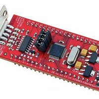
EA-QSB-102
Manufacturer Part Number
EA-QSB-102
Description
MCU, MPU & DSP Development Tools QUICKSTART PROTOTYPE BRD W/ LPC2106 RS232
Manufacturer
Embedded Artists
Specifications of EA-QSB-102
Processor To Be Evaluated
LPC2106
Data Bus Width
16 bit, 32 bit
Interface Type
RS-232, I2C, SPI, UART
Core
ARM7TDMI-S
Dimensions
27.9 mm x 65.3 mm
Maximum Operating Temperature
+ 85 C
Operating Supply Voltage
5 V
Lead Free Status / RoHS Status
Lead free / RoHS Compliant


NXP Semiconductors
Table 3.
LPC2104_2105_2106_7
Product data sheet
Symbol
P0.0 to P0.31
P0.0/TXD0/PWM1
P0.1/RXD0/PWM3
P0.2/SCL/CAP0.0
P0.3/SDA/MAT0.0
P0.4/SCK/CAP0.1
P0.5/MISO/MAT0.1
P0.6/MOSI/CAP0.2
P0.7/SSEL/PWM2
P0.8/TXD1/PWM4
P0.9/RXD1/PWM6
P0.10/RTS1/CAP1.0
Pin description
5.2 Pin description
Pin
13
14
18
21
22
23
24
28
29
30
35
[1]
[1]
[2]
[2]
[1]
[1]
[1]
[1]
[1]
[1]
[1]
Type
I/O
I/O
O
O
I/O
I
O
I/O
I/O
I
I/O
I/O
O
I/O
I/O
I
I/O
I/O
O
I/O
I/O
I
I/O
I
O
I/O
O
O
I/O
I
O
I/O
O
I
Description
Port 0: Port 0 is a 32-bit bidirectional I/O port with individual direction controls for
each bit. The operation of port 0 pins depends upon the pin function selected via
the Pin Connect Block.
P0.0 — Port 0 bit 0.
TXD0 — Transmitter output for UART 0.
PWM1 — Pulse Width Modulator output 1.
P0.1 — Port 0 bit 1.
RXD0 — Receiver input for UART 0.
PWM3 — Pulse Width Modulator output 3.
P0.2 — Port 0 bit 2. The output is open-drain.
SCL — I
CAP0.0 — Capture input for Timer 0, channel 0.
P0.3 — Port 0 bit 3. The output is open-drain.
SDA — I
MAT0.0 — Match output for Timer 0, channel 0. The output is open-drain.
P0.4 — Port 0 bit 4.
SCK — Serial clock for SPI/SSP
CAP0.1 — Capture input for Timer 0, channel 1.
P0.5 — Port 0 bit 5.
MISO — Master In Slave Out for SPI/SSP
data output from SPI/SSP slave.
MAT0.1 — Match output for Timer 0, channel 1.
P0.6 — Port 0 bit 6.
MOSI — Master Out Slave In for SPI/SSP
or data input to SPI/SSP slave.
CAP0.2 — Capture input for Timer 0, channel 2.
P0.7 — Port 0 bit 7.
SSEL — Slave Select for SPI/SSP
PWM2 — Pulse Width Modulator output 2.
P0.8 — Port 0 bit 8.
TXD1 — Transmitter output for UART 1.
PWM4 — Pulse Width Modulator output 4.
P0.9 — Port 0 bit 9.
RXD1 — Receiver input for UART 1.
PWM6 — Pulse Width Modulator output 6.
P0.10 — Port 0 bit 10.
RTS1 — Request to Send output for UART 1.
CAP1.0 — Capture input for Timer 1, channel 0.
Rev. 07 — 20 June 2008
2
2
C-bus clock input/output. Open-drain output (for I
C-bus data input/output. Open-drain output (for I
[3]
. Clock output from master or input to slave.
[3]
LPC2104/2105/2106
. Selects the SPI/SSP interface as a slave.
Single-chip 32-bit microcontrollers
[3]
[3]
. Data input to SPI/SSP master or
. Data output from SPI/SSP master
2
2
C-bus compliance).
C-bus compliance).
© NXP B.V. 2008. All rights reserved.
7 of 41
Related parts for EA-QSB-102
Image
Part Number
Description
Manufacturer
Datasheet
Request
R

Part Number:
Description:
MCU, MPU & DSP Development Tools QUICKSTART PROTOTYPE BRD W/ LPC2129 CAN
Manufacturer:
Embedded Artists
Datasheet:

Part Number:
Description:
MCU, MPU & DSP Development Tools QUICKSTART PROTOTYPE BRD
Manufacturer:
Embedded Artists
Datasheet:

Part Number:
Description:
MCU, MPU & DSP Development Tools LPC2148 USB QUICKSTART BRD
Manufacturer:
Embedded Artists
Datasheet:
Part Number:
Description:
MCU, MPU & DSP Development Tools LPC2129 CAN QUICKSTART BRD
Manufacturer:
Embedded Artists
Datasheet:
Part Number:
Description:
MCU, MPU & DSP Development Tools QUICKSTART PROTOTYPE BRD W/ LPC2148
Manufacturer:
Embedded Artists
Datasheet:

Part Number:
Description:
MCU, MPU & DSP Development Tools LPC2106 RS232 QUICKSTART BRD
Manufacturer:
Embedded Artists
Datasheet:

Part Number:
Description:
BOARD QUICK START LPC1343
Manufacturer:
Embedded Artists
Datasheet:

Part Number:
Description:
Development Boards & Kits - ARM QUICK START BOARD LPC11U35
Manufacturer:
Embedded Artists
Datasheet:
Part Number:
Description:
KIT LPC3141 SODIMM 66X48 200POS
Manufacturer:
Embedded Artists
Datasheet:
Part Number:
Description:
KIT LPC3152 SODIMM 66X48 200POS
Manufacturer:
Embedded Artists
Datasheet:
Part Number:
Description:
BOARD OEM W/LPC2478 MCU
Manufacturer:
Embedded Artists
Datasheet:
Part Number:
Description:
KIT LPC3250 259 WITH QVGA
Manufacturer:
Embedded Artists
Datasheet: