EA-QSB-102 Embedded Artists, EA-QSB-102 Datasheet - Page 16
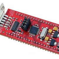
EA-QSB-102
Manufacturer Part Number
EA-QSB-102
Description
MCU, MPU & DSP Development Tools QUICKSTART PROTOTYPE BRD W/ LPC2106 RS232
Manufacturer
Embedded Artists
Specifications of EA-QSB-102
Processor To Be Evaluated
LPC2106
Data Bus Width
16 bit, 32 bit
Interface Type
RS-232, I2C, SPI, UART
Core
ARM7TDMI-S
Dimensions
27.9 mm x 65.3 mm
Maximum Operating Temperature
+ 85 C
Operating Supply Voltage
5 V
Lead Free Status / RoHS Status
Lead free / RoHS Compliant


NXP Semiconductors
LPC2104_2105_2106_7
Product data sheet
6.10.1 Features
6.9.1 Features
6.9.2 Features added with the Fast GPIO set of registers available on
6.10 UARTs
6.9 General purpose parallel I/O
Table 7.
Device pins that are not connected to a specific peripheral function are controlled by the
GPIO registers. Pins may be dynamically configured as inputs or outputs. Separate
registers allow setting or clearing any number of outputs simultaneously. The value of the
output register may be read back, as well as the current state of the port pins.
LPC2104/2105/2106/01 only
The LPC2104/2105/2106 each contain two UARTs. One UART provides a full modem
control handshake interface, the other provides only transmit and receive data lines.
PINSEL1
25:24
27:26
29:28
31:30
•
•
•
•
•
•
•
•
•
•
•
•
Direction control of individual bits.
Separate control of output set and clear.
All I/O default to inputs after reset.
Fast GPIO registers are relocated to the ARM local bus for the fastest possible I/O
timing, enabling port pin toggling up to 3.5 times faster than earlier LPC2000 devices.
Mask registers allow treating sets of port bits as a group, leaving other bits
unchanged.
All Fast GPIO registers are byte addressable.
Entire port value can be written in one instruction.
Ports are accessible via either the legacy group of registers (GPIOs) or the group of
registers providing accelerated port access (Fast GPIOs).
16 byte Receive and Transmit FIFOs
Register locations conform to 16C550 industry standard
Receiver FIFO trigger points at 1 B, 4 B, 8 B, and 14 B
Built-in baud rate generator
Pin function select register 1 (PINSEL1 - 0xE002 C004)
Pin name
P0.28
P0.29
P0.30
P0.31
Rev. 07 — 20 June 2008
Value
0
0
0
0
0
0
0
0
0
1
0
1
0
1
0
1
LPC2104/2105/2106
Function
GPIO Port 0.28
TMS
GPIO Port 0.29
TCK
GPIO Port 0.30
TDI
GPIO Port 0.31
TDO
Single-chip 32-bit microcontrollers
…continued
© NXP B.V. 2008. All rights reserved.
Value after
reset
0
0
0
0
16 of 41
Related parts for EA-QSB-102
Image
Part Number
Description
Manufacturer
Datasheet
Request
R

Part Number:
Description:
MCU, MPU & DSP Development Tools QUICKSTART PROTOTYPE BRD W/ LPC2129 CAN
Manufacturer:
Embedded Artists
Datasheet:

Part Number:
Description:
MCU, MPU & DSP Development Tools QUICKSTART PROTOTYPE BRD
Manufacturer:
Embedded Artists
Datasheet:

Part Number:
Description:
MCU, MPU & DSP Development Tools LPC2148 USB QUICKSTART BRD
Manufacturer:
Embedded Artists
Datasheet:
Part Number:
Description:
MCU, MPU & DSP Development Tools LPC2129 CAN QUICKSTART BRD
Manufacturer:
Embedded Artists
Datasheet:
Part Number:
Description:
MCU, MPU & DSP Development Tools QUICKSTART PROTOTYPE BRD W/ LPC2148
Manufacturer:
Embedded Artists
Datasheet:

Part Number:
Description:
MCU, MPU & DSP Development Tools LPC2106 RS232 QUICKSTART BRD
Manufacturer:
Embedded Artists
Datasheet:

Part Number:
Description:
BOARD QUICK START LPC1343
Manufacturer:
Embedded Artists
Datasheet:

Part Number:
Description:
Development Boards & Kits - ARM QUICK START BOARD LPC11U35
Manufacturer:
Embedded Artists
Datasheet:
Part Number:
Description:
KIT LPC3141 SODIMM 66X48 200POS
Manufacturer:
Embedded Artists
Datasheet:
Part Number:
Description:
KIT LPC3152 SODIMM 66X48 200POS
Manufacturer:
Embedded Artists
Datasheet:
Part Number:
Description:
BOARD OEM W/LPC2478 MCU
Manufacturer:
Embedded Artists
Datasheet:
Part Number:
Description:
KIT LPC3250 259 WITH QVGA
Manufacturer:
Embedded Artists
Datasheet: