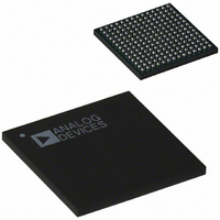
AD6634BBC Analog Devices Inc, AD6634BBC Datasheet - Page 20

AD6634BBC
Manufacturer Part Number
AD6634BBC
Description
IC,RF/Baseband Circuit,CMOS,BGA,196PIN,PLASTIC
Manufacturer
Analog Devices Inc
Series
AD6634r
Datasheet
1.AD6634BCPCB.pdf
(52 pages)
Specifications of AD6634BBC
Rohs Status
RoHS non-compliant
Rf Type
Cellular, CDMA2000, EDGE, GPRS, GSM
Number Of Mixers
1
Voltage - Supply
3 V ~ 3.6 V
Package / Case
196-CSPBGA
Current - Supply
-
Frequency
-
Gain
-
Noise Figure
-
Secondary Attributes
-
Lead Free Status / RoHS Status
Available stocks
Company
Part Number
Manufacturer
Quantity
Price
Company:
Part Number:
AD6634BBC
Manufacturer:
AD
Quantity:
13 888
Part Number:
AD6634BBC
Manufacturer:
ADI/亚德诺
Quantity:
20 000
AD6634
INPUT DATA PORTS
The AD6634 features dual high speed ADC input ports, input
port A and input port B. The dual input ports allow for the
most flexibility with a single tuner chip. These can be diversity
inputs or truly independent inputs such as separate antenna
segments. Either ADC port can be routed to one of four tuner
channels. For added flexibility, each input port can be used to
support multiplexed inputs such as those found on the AD6600
or other ADCs with multiplexed outputs. This added flexibility
can allow for up to four different analog sources to be processed
simultaneously by the four internal channels.
In addition, the front end of the AD6634 contains circuitry that
enables high speed signal level detection and control. This is
accomplished with a unique high speed level detection circuit
that offers minimal latency and maximum flexibility to control
up to four analog signal paths. The overall signal path latency
from input to output on the AD6634 can be expressed in high
speed clock cycles. The following equation can be used to
calculate the latency.
M
filters, respectively. N
Input Data Format
Each input port consists of a 14-bit mantissa and 3-bit exponent.
If interfacing to a standard ADC is required, the exponent bits can
be grounded. If connected to a floating point ADC such as the
AD6600, the exponent bits from that product can be connected
to the input exponent bits of the AD6634. The mantissa data
format is two’s complement and the exponent is unsigned binary.
Input Timing
The data from each high speed input port is latched on the
rising edge of CLK. This clock signal is used to sample the
input port and clock the synchronous signal processing stages
that follow in the selected channels.
The clock signals can operate up to 80 MHz and have a 50% duty
cycle. In applications using high speed ADCs, the ADC sample
clock or data valid strobe is typically used to clock the AD6634.
EXP[2:0]
IN[13:0]
rCIC2
CLK
and M
Figure 25. Input Data Timing Requirements
T
LATENCY
CIC5
are decimation values for the rCIC2 and CIC5
=
TAPS
M
rCIC
is the number RCF taps chosen.
2
(
M
t
SI
CIC
DATA
5
+
t
HI
7
)
+
N
TAPS
+
26
–20–
Input Enable Control
There is an IENA and an IENB pin for Input Port A and Input
Port B, respectively. There are four modes of operation possible
while using each IEN pin. Using these modes, it is possible to
emulate operation of the other RSPs, such as the AD6620,
which offer dual channel modes normally associated with diver-
sity operations. These modes are: IEN transition to Low, IEN
transition to High, IEN High, and Blank on IEN low.
In the IEN High mode, the inputs and normal operations occur
when the input enable is high. In the IEN transition to Low mode,
normal operations occur on the first rising edge of the clock after
the IEN transitions to low. Likewise in the IEN transition to High
mode, operations occur on the rising edge of the clock after the
IEN transitions to High. (See the Numerically Controlled Oscil-
lator section for more details on configuring the Input Enable
Modes.) In Blank on IEN low mode, the input data is interpreted
as zero when IEN is low.
A typical application for this feature would be to take the data
from an AD6600 Diversity ADC to one of the inputs of the
AD6634. The A/B_OUT from that chip would be tied to the
IEN. Then one channel within the AD6634 would be set so that
IEN transition to Low is enabled. Another channel would be
configured so that IEN transition to High is enabled. This would
allow two of the AD6634 channels to be configured to emulate
that AD6620 in diversity mode. Of course the NCO frequencies
and other channel characteristics would need to be set similarly,
but this feature allows the AD6634 to handle interleaved data
streams such as those found on the AD6600.
The difference between the IEN transition to high and the IEN
high is found when a system clock is provided that is higher than
the data rate of the converter. It is often advantageous to supply
a clock that runs faster than the data rate so that additional filter
taps can be computed. This naturally provides better filtering.
In order to ensure that other parts of the circuit properly recog-
nize the faster clock in the simplest manner, the IEN transition
to low or high should be used. In this mode, only the first clock
edge that meets the setup and hold times will be used to latch
and process the input data. All other clock pulses are ignored by
front end processing. However, each clock cycle will still produce
a new filter computation pair.
CLK
Figure 26. CLK Timing Requirements
t
CLKL
t
CLK
t
CLKH
REV. 0


