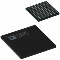
AD6634BBC Analog Devices Inc, AD6634BBC Datasheet - Page 8

AD6634BBC
Manufacturer Part Number
AD6634BBC
Description
IC,RF/Baseband Circuit,CMOS,BGA,196PIN,PLASTIC
Manufacturer
Analog Devices Inc
Series
AD6634r
Datasheet
1.AD6634BCPCB.pdf
(52 pages)
Specifications of AD6634BBC
Rohs Status
RoHS non-compliant
Rf Type
Cellular, CDMA2000, EDGE, GPRS, GSM
Number Of Mixers
1
Voltage - Supply
3 V ~ 3.6 V
Package / Case
196-CSPBGA
Current - Supply
-
Frequency
-
Gain
-
Noise Figure
-
Secondary Attributes
-
Lead Free Status / RoHS Status
Available stocks
Company
Part Number
Manufacturer
Quantity
Price
Company:
Part Number:
AD6634BBC
Manufacturer:
AD
Quantity:
13 888
Part Number:
AD6634BBC
Manufacturer:
ADI/亚德诺
Quantity:
20 000
AD6634
GENERAL TIMING CHARACTERISTICS
Parameter (Conditions)
CLK TIMING REQUIREMENTS
RESET TIMING REQUIREMENTS
INPUT WIDEBAND DATA TIMING REQUIREMENTS
LEVEL INDICATOR OUTPUT SWITCHING CHARACTERISTICS
SYNC TIMING REQUIREMENTS
SERIAL PORT CONTROL TIMING REQUIREMENTS
SWITCHING CHARACTERISTICS
INPUT CHARACTERISTICS
PARALLEL PORT TIMING REQUIREMENTS (MASTER MODE)
SWITCHING CHARACTERISTICS
INPUT CHARACTERISTICS
PARALLEL PORT TIMING REQUIREMENTS (SLAVE MODE)
SWITCHING CHARACTERISTICS
INPUT CHARACTERISTICS
LINK PORT TIMING REQUIREMENTS
SWITCHING CHARACTERISTICS
NOTES
1
2
3
Specifications subject to change without notice.
All Timing Specifications valid over VDD range of 2.25 V to 2.75 V and VDDIO range of 3.0 V to 3.6 V.
C
The timing parameters for Px[15:0], PxREQ, PxACK, LxCLKOUT, Lx[7:0] apply for port A and B (x stands for A or B).
LOAD
t
t
t
t
t
t
t
t
t
t
t
t
t
t
t
t
t
t
t
t
t
t
t
t
t
t
t
t
t
t
t
CLK
CLKL
CLKH
RESL
SI
HI
DLI
SS
HS
SCLK
SCLKL
SCLKH
SSI
HSI
DPOCLKL
DPOCLKLL
DPREQ
DPP
SPA
HPA
POCLK
POCLKL
POCLKH
DPREQ
DPP
SPA
HPA
RDLCLK
FDLCLK
RLCLKDAT
FLCLKDAT
= 40 pF on all outputs unless otherwise specified
CLK Period
CLK Width Low
CLK Width High
RESET Width Low
Input to ↑CLK Setup Time
Input to ↑CLK Hold Time
↑CLK to LI (A–A, B; B–A, B) Output Delay Time
SYNC (A, B, C, D) to ↑CLK Setup Time
SYNC (A, B, C, D) to ↑CLK Hold Time
SCLK Period
SCLK Low Time
SCLK High Time
SDI to ↓SCLK Setup Time
SDI to ↓SCLK Hold Time
↓CLK to ↑PCLK Delay (Divide by 1)
↓CLK to ↑PCLK Delay (Divide by 2, 4, or 8)
↑CLK to ↑PxREQ Delay
↑CLK to Px[15:0] Delay
PxACK to ↓PCLK Setup Time
PxACK to ↓PCLK Hold Time
PCLK Period
PCLK Low Period (when PCLK Divisor = 1)
PCLK High Period (when PCLK Divisor = 1)
↑CLK to ↑PxREQ Delay
↑CLK to Px[15:0] Delay
PxACK to ↓PCLK Setup Time
PxACK to ↓PCLK Hold Time
↑PCLK to ↑LxCLKOUT Delay
↓PCLK to ↓LxCLKOUT Delay
↑LCLKOUT to Lx[7:0] Delay
↓LCLKOUT to Lx[7:0] Delay
2
3
3
3
1, 2
–8–
Temp
Full
Full
Full
Full
Full
Full
Full
Full
Full
Full
Full
Full
Full
Full
Full
Full
Full
Full
Full
Full
Full
Full
Full
Test
Level
I
IV
IV
I
IV
IV
IV
IV
IV
IV
IV
IV
IV
IV
IV
IV
I
IV
IV
IV
IV
IV
IV
Min
12.5
5.6
5.6
30.0
2.0
1.0
3.3
2.0
1.0
16
3.0
3.0
1.0
1.0
6.5
8.3
+7.0
–3.0
12.5
2.0
2.0
1.0
1.0
0
0
AD6634BBC
Typ
0.5 × t
0.5 × t
0.5 × t
0.5 × t
CLK
CLK
POCLK
POCLK
Max
10.0
10.5
14.6
1.0
0.0
10.0
11.0
2.5
0
2.9
2.2
REV. 0
Unit
ns
ns
ns
ns
ns
ns
ns
ns
ns
ns
ns
ns
ns
ns
ns
ns
ns
ns
ns
ns
ns
ns
ns
ns
ns
ns
ns
ns
ns
ns
ns


