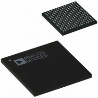
AD6634BBC Analog Devices Inc, AD6634BBC Datasheet - Page 28

AD6634BBC
Manufacturer Part Number
AD6634BBC
Description
IC,RF/Baseband Circuit,CMOS,BGA,196PIN,PLASTIC
Manufacturer
Analog Devices Inc
Series
AD6634r
Datasheet
1.AD6634BCPCB.pdf
(52 pages)
Specifications of AD6634BBC
Rohs Status
RoHS non-compliant
Rf Type
Cellular, CDMA2000, EDGE, GPRS, GSM
Number Of Mixers
1
Voltage - Supply
3 V ~ 3.6 V
Package / Case
196-CSPBGA
Current - Supply
-
Frequency
-
Gain
-
Noise Figure
-
Secondary Attributes
-
Lead Free Status / RoHS Status
Available stocks
Company
Part Number
Manufacturer
Quantity
Price
Company:
Part Number:
AD6634BBC
Manufacturer:
AD
Quantity:
13 888
Part Number:
AD6634BBC
Manufacturer:
ADI/亚德诺
Quantity:
20 000
AD6634
For RCF Scale of 0, Scaling Factor is equal to –18.06 dB, and for
maximum RCF Scale of 15, Scaling Factor is equal to 72.25 dB.
If Bit 7 is set, the same exponent will be used for both the real
and imaginary (I and Q) outputs. The exponent used will be the
one that prevents numeric overflow at the expense of small
signal accuracy. However, this is seldom a problem as small
numbers would represent 0 regardless of the exponent used.
Bit 8 is the RCF bank select bit used to program the register. When
this bit is 0, the lowest block of 128 is selected (taps 0 through
127). When high, the highest block is selected (taps 128 through
255). It should be noted that while the chip is computing filters,
tap 127 is adjacent to 128 and there are no paging issues.
Bit 9 selects where the input to each RCF originates. If Bit 9 is clear,
the RCF input comes from the CIC5 normally associated with
the RCF. If, however, the bit is set, the input comes from CIC5
channel 1. The only exception is channel 1, which uses the output
of CIC5 channel 0 as its alternate. Using this feature, each RCF
can operate on its own channel data or be paired with the RCF
of channel 1. The RCF of channel 1 can also be paired with chan-
nel 0. This control bit is used with polyphase distributed filtering.
If Bit 10 is clear, the AD6634 channel operates in normal mode.
However, if Bit 10 is set, the RCF is bypassed to Channel BIST.
See the BIST (Built-In Self-Test) section for more details.
INTERPOLATING HALF-BAND FILTERS
The AD6634 has two interpolating half-band finite impulse
response filters that immediately precede the two digital AGCs
and follow the four RCF channel outputs. Each interpolating
half-band takes 16-bit I and 16-bit Q data from the preceding
RCF and outputs 16-bit I and 16-bit Q to the AGC. The half-band
and AGC operate independently of each other, so the AGC can
be bypassed, in which case the output of the half-band is sent
directly to the output data port. The half-bands also operate
independently of each other—either one can be enabled or
disabled. The control register for half-band A is at address 0x08
and for half-band B, address 0x09.
Half-band filters also perform the function of interleaving data
from various RCF channel outputs prior to the actual function
of interpolation. This interleaving of data is allowed even when
the actual function of Half-band filter is bypassed. This feature
allows for the usage of multiple channels (implementing a
polyphase filter) on the AD6634 to process a single carrier. Either
RCF phase decimation or start hold-off counter for the channels
is used to appropriately phase the channels. For example, if two
channels of AD6634 are used to process one CDMA2000 carrier,
RCF filters for both the channels should be 180° out of phase.
This can be done using RCF phase decimation or an appropriate
start hold-off counter followed by appropriate NCO phase offsets.
Half-band A can listen to all four channels: 0, 1, 2, and 3; channel
0 and 1; or only channel 0. Half-band B can listen to channels 2
and 3, or only channel 2. Each half-band interleaves the channels
specified in its control register and interpolates by 2 on the
combined data from those channels. For one channel running at
twice the chip rate, the half-band can be used to output channel
data at 43 the chip rate.
With respect to the chip rate, the frequency response of the
interpolating half-band FIR is shown in Figure 32.
–28–
The SNR of the interpolating half-band is around –149.6 dB.
The highest error spurs due to fixed-point arithmetic are around
–172.9 dB. The coefficients of the 13-tap interpolating half-band
FIR are given in the Table VII.
AUTOMATIC GAIN CONTROL
The AD6634 is equipped with two independent automatic gain
control (AGC) loops for direct interface with a RAKE receiver.
Each AGC circuit has 96 dB of range. It is important that the
decimating filters of the AD6634 preceding the AGC reject
undesired signals, so that each AGC loop is only operating on
the carrier of interest and carriers at other frequencies do not
affect the ranging of the loop.
The AGC compresses the 23-bit complex output from the inter-
polating half-band filter into a programmable word size of 4–8,
10, 12, or 16 bits. Since the small signals from the lower bits are
pushed into higher bits by adding gain, the clipping of the lower
bits does not compromise the SNR of the signal of interest. The
AGC maintains a constant mean power on the output despite the
level of the signal of interest, allowing operation in environments
where the dynamic range of the signal exceeds the dynamic range
of the output resolution.
Figure 32. Interpolating Half-Band Frequency Response
–10
–20
–30
–40
–50
–60
–70
–80
0
0
Table VII. Half-Band Coefficients
0.5
1.0
SPECTRUM OF HALF-BAND
MULTIPLES OF CHIP RATE
1.5
N
0
14
0
–66
0
309
512
309
0
–66
0
14
0
i
f
CHIP
2.0
f
SAMP
2.5
3.0
3.5
f
f
SAMP
CHIP
4.0
REV. 0


