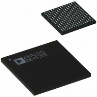
AD6634BBC Analog Devices Inc, AD6634BBC Datasheet - Page 39

AD6634BBC
Manufacturer Part Number
AD6634BBC
Description
IC,RF/Baseband Circuit,CMOS,BGA,196PIN,PLASTIC
Manufacturer
Analog Devices Inc
Series
AD6634r
Datasheet
1.AD6634BCPCB.pdf
(52 pages)
Specifications of AD6634BBC
Rohs Status
RoHS non-compliant
Rf Type
Cellular, CDMA2000, EDGE, GPRS, GSM
Number Of Mixers
1
Voltage - Supply
3 V ~ 3.6 V
Package / Case
196-CSPBGA
Current - Supply
-
Frequency
-
Gain
-
Noise Figure
-
Secondary Attributes
-
Lead Free Status / RoHS Status
Available stocks
Company
Part Number
Manufacturer
Quantity
Price
Company:
Part Number:
AD6634BBC
Manufacturer:
AD
Quantity:
13 888
Part Number:
AD6634BBC
Manufacturer:
ADI/亚德诺
Quantity:
20 000
0x90: rCIC2 Decimation – 1 (M
This register is used to set the decimation in the rCIC2 filter.
The value written to this register is the decimation minus one.
The rCIC2 decimation can range from 1 to 4096, depending
upon the interpolation of the channel. The decimation must
always be greater than the interpolation. M
larger than L
rCIC2 scalar can be chosen. For more details, the rCIC2 section
should be consulted.
0x91: rCIC2 Interpolation – 1 (L
This register is used to set the interpolation in the rCIC2 filter.
The value written to this register is the interpolation minus one.
The rCIC2 interpolation can range from 1 to 512, depending
upon the decimation of the rCIC2. There is no timing error
associated with this interpolation. See the rCIC2 section for
further details.
REV. 0
Channel
Address
90
91
92
93
94
95
96
97–9F
A0
A1
A2
A3
A4
A5
A6
A7
A8
A9
rCIC2
and both must be chosen such that a suitable
Register
rCIC2 Decimation – 1
rCIC2 Decimation – 1
rCIC2 Scale
Reserved
CIC5 Decimation – 1
CIC5 Scale
Reserved
Unused
RCF Decimation – 1
RCF Decimation Phase
RCF Number of Taps – 1
RCF Coefficient Offset
RCF Control Register
BIST Signature for I Path
BIST Signature for Q Path
No. of BIST Outputs to
Accumulate
RAM BIST Control Register
Output Control Register
rCIC2
rCIC2
– 1)
– 1)
rCIC2
Table XI. Channel Address Memory Map
must be chosen
–39–
Bit
Width
12
9
12
8
8
5
8
8
8
8
8
11
16
16
20
3
0x92: rCIC2 Scale
The rCIC2 scale register is used to provide attenuation to com-
pensate for the gain of the rCIC2 and to adjust the linearization
of the data from the floating-point input. The use of this scale
register is influenced both by the rCIC2 growth and floating-
point input port considerations. The rCIC2 section should be
consulted for details. The rCIC2 scalar has been combined with
the exponent offset and will need to be handled appropriately in
both the input port and rCIC2 sections.
Bit 11 determines the polarity of the exponent. Normally, this
bit will be cleared unless an ADC such as the AD6600 is used,
in which case this bit will be set.
Bit 10 determines the weight of the exponent word associated
with the input port. When this bit is Low, each exponent step is
considered to be worth 6.02 dB. When this bit is High, each
exponent step is considered to be worth 12.02 dB.
Comments
M
L
11: Exponent Invert
10: Exponent Weight
9–5: rCIC2_QUIET[4:0]
4–0: rCIC2_LOUD[4:0]
Reserved (Must Be Written Low)
M
4–0: CIC5_SCALE[4:0]
Reserved (Must Be Written Low)
M
P
N
CO
10: RCF Bypass BIST
9: RCF Input Select
(Own 0, Other 1)
8: Program RAM Bank 1/0
7: Use Common Exponent
6: Force Output Scale
5–4: Output Format
3–0:1Output Scale
BIST-I
BIST-Q
19–0: No. of Outputs(Counter Value Read)
2: D-RAM Fail/Pass
1: NC-RAM Fail/Pass
0: RAM BIST Enable
9: Map RCF Data to BIST Registers
5: Output Format
RCF
rCIC2
TAPS
rCIC2
CIC5
RCF
1x: Floating Point 12 + 4
01: Floating Point 8 + 4
00: Fixed Point
1:16-Bit I and 16-Bit Q
0:12-Bit I and 12-Bit Q
RCF
–1
–1
–1
–1
–1
AD6634


