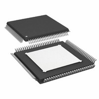
AD9445BSVZ-105 Analog Devices Inc, AD9445BSVZ-105 Datasheet - Page 11

AD9445BSVZ-105
Manufacturer Part Number
AD9445BSVZ-105
Description
IC,A/D CONVERTER,SINGLE,14-BIT,BICMOS,TQFP,100PIN
Manufacturer
Analog Devices Inc
Datasheet
1.AD9445BSVZ-105.pdf
(40 pages)
Specifications of AD9445BSVZ-105
Design Resources
Using AD8376 to Drive Wide Bandwidth ADCs for High IF AC-Coupled Appls (CN0002) Using AD8352 as an Ultralow Distortion Differential RF/IF Front End for High Speed ADCs (CN0046) Using ADL5562 Differential Amplifier to Drive Wide Bandwidth ADCs for High IF AC-Coupled Appls (CN0110)
Number Of Bits
14
Sampling Rate (per Second)
105M
Data Interface
Parallel
Number Of Converters
1
Power Dissipation (max)
2.4W
Voltage Supply Source
Single Supply
Operating Temperature
-40°C ~ 85°C
Mounting Type
Surface Mount
Package / Case
100-TQFP Exposed Pad
Lead Free Status / RoHS Status
Lead free / RoHS Compliant
Available stocks
Company
Part Number
Manufacturer
Quantity
Price
Company:
Part Number:
AD9445BSVZ-105
Manufacturer:
ADI
Quantity:
131
Company:
Part Number:
AD9445BSVZ-105
Manufacturer:
Analog Devices Inc
Quantity:
10 000
Table 7. Pin Function Descriptions—100-Lead TQFP/EP in LVDS Mode
Pin No.
1
2, 49 to 52
3
4
5
6, 18 to 20, 32 to 34, 36, 38,
43 to 45, 92 to 97
7
8
9, 21, 24, 39, 42, 46, 91, 98, 99,
Exposed Heat Sink
10
11
12 to 17, 25 to 31, 35, 37
22
23
40
41
47, 63, 75, 87
48, 64, 76, 88
53
54
55
56
57
58
59
60
61
62
65
66
67
68
69
70
71
72
73
74
77
78
79
80
81
82
Mnemonic
DCS MODE
DNC
OUTPUT MODE
DFS
LVDS_BIAS
AVDD1
SENSE
VREF
AGND
REFT
REFB
AVDD2
VIN+
VIN−
CLK+
CLK−
DRGND
DRVDD
D0− (LSB)
D0+
D1−
D1+
D2−
D2+
D3−
D3+
D4−
D4+
D5−
D5+
DCO−
DCO+
D6−
D6+
D7−
D7+
D8−
D8+
D9−
D9+
D10−
D10+
D11−
D11+
Description
Clock Duty Cycle Stabilizer (DCS) Control Pin. CMOS compatible. DCS = low (AGND) to
enable DCS (recommended); DCS = high (AVDD1) to disable DCS.
Do Not Connect. These pins should float.
CMOS-Compatible Output Logic Mode Control Pin. OUTPUT MODE = 0 for CMOS mode;
OUTPUT MODE = 1 (AVDD1) for LVDS outputs.
Data Format Select Pin. CMOS control pin that determines the format of the output data.
DFS = high (AVDD1) for twos complement; DFS = low (ground) for offset binary format.
Set Pin for LVDS Output Current. Place 3.7 kΩ resistor terminated to DRGND.
3.3 V (±5%) Analog Supply.
Reference Mode Selection. Connect to AGND for internal 1 V reference; connect to
AVDD1 for external reference.
1.0 V Reference I/O. Function dependent on SENSE and external programming resistors.
Decouple to ground with 0.1 μF and 10 μF capacitors.
Analog Ground. The exposed heat sink on the bottom of the package must be
connected to AGND.
Differential Reference Output. Decoupled to ground with 0.1 μF capacitor and to REFB
(Pin 14) with 0.1 μF and 10 μF capacitors.
Differential Reference Output. Decoupled to ground with a 0.1 μF capacitor and to REFT
(Pin 13) with 0.1 μF and 10 μF capacitors.
5.0 V Analog Supply (±5%).
Analog Input—True.
Analog Input—Complement.
Clock Input—True.
Clock Input—Complement.
Digital Output Ground.
3.3 V Digital Output Supply (3.0 V to 3.6 V).
D0 Complement Output Bit (LVDS Levels).
D0 True Output Bit.
D1 Complement Output Bit.
D1 True Output Bit.
D2 Complement Output Bit.
D2 True Output Bit.
D3 Complement Output Bit.
D3 True Output Bit.
D4 Complement Output Bit.
D4 True Output Bit.
D5 Complement Output Bit.
D5 True Output Bit.
Data Clock Output—Complement.
Data Clock Output—True.
D6 Complement Output Bit.
D6 True Output Bit.
D7 Complement Output Bit.
D7 True Output Bit.
D8 Complement Output Bit.
D8 True Output Bit.
D9 Complement Output Bit.
D9 True Output Bit.
D10 Complement Output Bit.
D10 True Output Bit.
D11 Complement Output Bit.
D11 True Output Bit.
Rev. 0 | Page 11 of 40
AD9445


