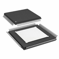
AD9445BSVZ-105 Analog Devices Inc, AD9445BSVZ-105 Datasheet - Page 25

AD9445BSVZ-105
Manufacturer Part Number
AD9445BSVZ-105
Description
IC,A/D CONVERTER,SINGLE,14-BIT,BICMOS,TQFP,100PIN
Manufacturer
Analog Devices Inc
Datasheet
1.AD9445BSVZ-105.pdf
(40 pages)
Specifications of AD9445BSVZ-105
Design Resources
Using AD8376 to Drive Wide Bandwidth ADCs for High IF AC-Coupled Appls (CN0002) Using AD8352 as an Ultralow Distortion Differential RF/IF Front End for High Speed ADCs (CN0046) Using ADL5562 Differential Amplifier to Drive Wide Bandwidth ADCs for High IF AC-Coupled Appls (CN0110)
Number Of Bits
14
Sampling Rate (per Second)
105M
Data Interface
Parallel
Number Of Converters
1
Power Dissipation (max)
2.4W
Voltage Supply Source
Single Supply
Operating Temperature
-40°C ~ 85°C
Mounting Type
Surface Mount
Package / Case
100-TQFP Exposed Pad
Lead Free Status / RoHS Status
Lead free / RoHS Compliant
Available stocks
Company
Part Number
Manufacturer
Quantity
Price
Company:
Part Number:
AD9445BSVZ-105
Manufacturer:
ADI
Quantity:
131
Company:
Part Number:
AD9445BSVZ-105
Manufacturer:
Analog Devices Inc
Quantity:
10 000
External Reference Operation
The AD9445’s internal reference is trimmed to enhance the gain
accuracy of the ADC. An external reference may be more stable
over temperature, but the gain of the ADC is not likely to improve.
Figure 49 shows the typical drift characteristics of the internal
reference in both 1 V and 0.5 V modes.
When the SENSE pin is tied to AVDD, the internal reference is
disabled, allowing the use of an external reference. An internal
reference buffer loads the external reference with an equivalent
7 kΩ load. The internal buffer still generates the positive and
negative full-scale references, REFT and REFB, for the ADC
core. The input span is always twice the value of the reference
voltage; therefore, the external reference must be limited to a
maximum of 1.6 V.
Analog Inputs
As with most new high speed, high dynamic range ADCs, the
analog input to the AD9445 is differential. Differential inputs
improve on-chip performance because signals are processed
through attenuation and gain stages. Most of the improvement
is a result of differential analog stages having high rejection of
even-order harmonics. There are also benefits at the PCB level.
First, differential inputs have high common-mode rejection of
stray signals, such as ground and power noise. Second, they
provide good rejection of common-mode signals, such as local
oscillator feedthrough. The specified noise and distortion of the
AD9445 cannot be realized with a single-ended analog input, so
such configurations are discouraged. Contact sales for
recommendations of other 14-bit ADCs that support single-
ended analog input configurations.
With the 1 V reference, which is the nominal value (see the
Internal Reference Trim section), the differential input range of
the AD9445 analog input is nominally 2.0 V p-p or 1.0 V p-p on
each input (VIN+ or VIN−).
The AD9445 analog input voltage range is offset from ground
by 3.5 V. Each analog input connects through a 1 kΩ resistor to
the 3.5 V bias voltage and to the input of a differential buffer.
The internal bias network on the input properly biases the
buffer for maximum linearity and range (see the
Circuits section).
Equivalent
Rev. 0 | Page 25 of 40
Therefore, the analog source driving the AD9445 should be ac-
coupled to the input pins. The recommended method for driving
the analog input of the AD9445 is to use an RF transformer to
convert single-ended signals to differential (see
Series resistors between the output of the transformer and the
AD9445 analog inputs help isolate the analog input source from
switching transients caused by the internal sample-and-hold
circuit. The series resistors, along with the 1 kΩ resisters connected
to the internal 3.5 V bias, must be considered in impedance
matching the transformer input. For example, if R
51 Ω, R
former, the input will match a 50 Ω source with a full-scale drive
of 10.0 dBm. The 50 Ω impedance matching can also be incor-
porated on the secondary side of the transformer, as shown in
the evaluation board schematic (see Figure 67).
High IF Applications
In applications where the analog input frequency range is
>100 MHz, the phase and amplitude matching at the analog
inputs becomes critical to optimize performance of the ADC.
The circuit in Figure 63 can be used to optimize the matching of
these parameters. This configuration uses a double balun config-
uration that has low parasitics, high bandwidth, and parasitic
cancellation.
SOURCE
1V p-p
50 Ω
CT
ETC1–1–13
S
Figure 61. Differential Analog Input Range for VREF = 1.0 V
is set to 33 Ω, and there is a 1:1 impedance ratio trans-
ANALOG
Figure 63. Double Balun-Coupled Analog Input Circuit
VIN+
VIN–
Figure 62. Transformer-Coupled Analog Input Circuit
SIGNAL
INPUT
DIGITAL OUT = ALL 1s
R
T
0.1 μ F
ETC1–1–13
ADT1–1WT
25 Ω
25 Ω
0.1 μF
R
R
DIGITAL OUT = ALL 0s
S
S
0.1 μF
VIN+
VIN–
AD9445
33 Ω
33 Ω
Figure 62).
T
is set to
VIN+
AD9445
VIN–
AD9445
3.5V


