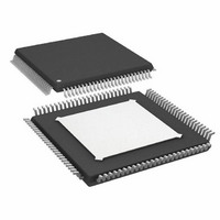
AD9445BSVZ-105 Analog Devices Inc, AD9445BSVZ-105 Datasheet - Page 8

AD9445BSVZ-105
Manufacturer Part Number
AD9445BSVZ-105
Description
IC,A/D CONVERTER,SINGLE,14-BIT,BICMOS,TQFP,100PIN
Manufacturer
Analog Devices Inc
Datasheet
1.AD9445BSVZ-105.pdf
(40 pages)
Specifications of AD9445BSVZ-105
Design Resources
Using AD8376 to Drive Wide Bandwidth ADCs for High IF AC-Coupled Appls (CN0002) Using AD8352 as an Ultralow Distortion Differential RF/IF Front End for High Speed ADCs (CN0046) Using ADL5562 Differential Amplifier to Drive Wide Bandwidth ADCs for High IF AC-Coupled Appls (CN0110)
Number Of Bits
14
Sampling Rate (per Second)
105M
Data Interface
Parallel
Number Of Converters
1
Power Dissipation (max)
2.4W
Voltage Supply Source
Single Supply
Operating Temperature
-40°C ~ 85°C
Mounting Type
Surface Mount
Package / Case
100-TQFP Exposed Pad
Lead Free Status / RoHS Status
Lead free / RoHS Compliant
Available stocks
Company
Part Number
Manufacturer
Quantity
Price
Company:
Part Number:
AD9445BSVZ-105
Manufacturer:
ADI
Quantity:
131
Company:
Part Number:
AD9445BSVZ-105
Manufacturer:
Analog Devices Inc
Quantity:
10 000
AD9445
ABSOLUTE MAXIMUM RATINGS
Table 5.
Parameter
ELECTRICAL
ENVIRONMENTAL
ESD CAUTION
ESD (electrostatic discharge) sensitive device. Electrostatic charges as high as 4000 V readily accumulate on
the human body and test equipment and can discharge without detection. Although this product features
proprietary ESD protection circuitry, permanent damage may occur on devices subjected to high energy
electrostatic discharges. Therefore, proper ESD precautions are recommended to avoid performance
degradation or loss of functionality.
AVDD1
AVDD2
DRVDD
AGND
AVDD1
AVDD2
AVDD2
D0± to D13±
CLK+/CLK−
OUTPUT MODE, DCS
VIN+, VIN−
VREF
SENSE
REFT, REFB
Storage Temperature
Operating Temperature
Lead Temperature
Junction Temperature
MODE, DFS, SFDR,
RF ENABLE
Range
Range
(Soldering 10 sec)
With
Respect
To
AGND
AGND
DGND
DGND
DRVDD
DRVDD
AVDD1
DGND
AGND
AGND
AGND
AGND
AGND
AGND
Rating
−0.3 V to +4 V
−0.3 V to +6 V
−0.3 V to +4 V
−0.3 V to +0.3 V
−4 V to +4 V
−4 V to +6 V
−4 V to +6 V
–0.3 V to DRVDD + 0.3 V
–0.3 V to AVDD1 + 0.3 V
–0.3 V to AVDD1 + 0.3 V
–0.3 V to AVDD2 + 0.3 V
–0.3 V to AVDD1 + 0.3 V
–0.3 V to AVDD1 + 0.3 V
–0.3 V to AVDD1 + 0.3 V
–65°C to +125°C
–40°C to +85°C
300°C
150°C
Rev. 0 | Page 8 of 40
Stresses above those listed under Absolute Maximum Ratings
may cause permanent damage to the device. This is a stress
rating only; functional operation of the device at these or any
other conditions above those indicated in the operational
section of this specification is not implied. Exposure to absolute
maximum rating conditions for extended periods may affect
device reliability.
THERMAL RESISTANCE
The heat sink of the AD9445 package must be soldered to ground.
Table 6.
Package Type
100-lead TQFP/EP
Typical θ
board in still air.
Typical θ
in still air.
Typical θ
the thermal resistance through heat sink path.
Airflow increases heat dissipation, effectively reducing θ
more metal directly in contact with the package leads from
metal traces through holes, ground, and power planes reduces
the θ
the ground plane.
JA
. It is required that the exposed heat sink be soldered to
JA
JB
JC
= 8.3°C/W (heat sink soldered) for multilayer board
= 19.8°C/W (heat sink soldered) for multilayer
= 2°C/W (junction to exposed heat sink) represents
θ
19.8
JA
θ
8.3
JB
θ
2
JC
Unit
°C/W
JA
. Also,


